Tutorial 9: Creating a
Custom Block for Synthesis,
Place & Route
This material is by Steven Levitan and Bo Zhao for the environment at the
University of Pittsburgh, 2008/2009.
·
Updated
17-Feb-2010 by Bo Zhao
We are using the NCSU/OSU FreePDK, Synopsys Design Compiler, Encounter 7.1, and Virtuoso 1.6.1.2
Please consult the NCSU EDA Wiki for background information
Many thanks to the team at NCSU and Oklahoma State University
Please see our tutorial on setting up the design environment and running Virtuoso
Before you get started, you should understand that these tools are very powerful and have lots of options. What we are showing here is one simple path through the design flow. To understand the tools, and their power, you must explore their capabilities by reading the help manuals, and trying lots of tests. Use the configuration files and scripts to keep your work manageable, and keep notes about what works, and what does not, so you don't make the same mistakes over and over.
Similar to a standard cell library, a custom block typically need to provide several files to the synthesis and P&R tools to identify all the different aspects (physical, electrical, functional) of the design. The .lib file describes the timing information, and the .db file is simply compiled from .lib file for Synopsys Design Compiler. The .lef file describes the layout information. And the Verilog (VHDL is also usually provided) file captures the functional behavior. This may also have a timing description of the block, which should be compiled before simulating a design that utilizes this block.
Before preparing these files, a great amount of effort should be spent on custom designs from transistors, gates, to module/block. The custom block should be fully tested with SPICE level simulations, fully layed out and should have passed DRC, LVS, and also fully verified after extraction. You want to make a reliable well tested component before you try to use it.
In this tutorial we use a small custom SRAM array as an example, which contains 64*32 SRAM cells (64 words, 32 bits per word), 32 write and precharge circuits, and 32 read circuits (no row decoder included). It was built in Virtuoso, extracted with Calibre, and simulated with HSPICE.
1. LEF file generation
Make a copy of your design library, because the abstract procedure may write to the original library. It is recommended that you create a separate folder for the abstract model and copy your design library there. In this tutorial we will use the memory component that is in the $CLASS directory. That component is itself a complete hierarchical design from virtuoso with schematics, layout and symbol views. We start by making a copy
> mkdir
abstract
> cp -r $CLASS/memory
abstract/
Go to your abstract directory, setup your environment, and start Virtuoso.
> cd
abstract
> setup_all
> virtuoso &
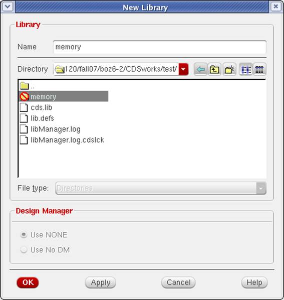
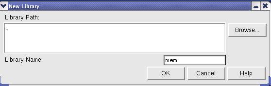
Open the Library Manager, and click File -> New -> Library... In the pop-up window, click the folder of the copied design library, and fill in the name as the folder name, then click OK.
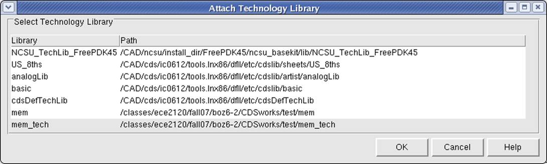
In next window, choose "Attach to an existing technology library", then OK. Next, choose "NCSU_TechLib_FreePDK45", click OK.
Because the abstractor will write to the technology library to which your design library is attached, and the current tech lib is read only, we next need to make a writable copy of the tech lib, and attach your design lib to it.
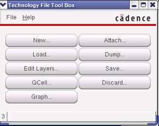
In the virtuoso main window (Command Interpreter Window, CIW), click Tools -> Technology File Manager... click New...
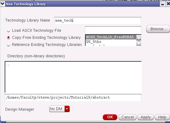
Fill in the tech lib name
(e.g. mem_tech). Choose
"Copy From Existing Technology Library" and make sure
"NCSU_TechLib_FreePDK45" is selected, then
click OK.
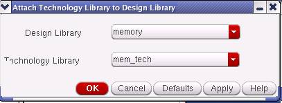
Back to the "Technology File Tool Box" window, hit
the Attach... button. Then select your design lib (e.g. memory) and the new
tech lib (e.g. mem_tech), click OK.
1.2 Stream out GDSII file
In CIW, click File -> Export ->
Stream..., then click OK (Stmout From
Disk).
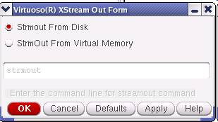
Fill in the gds file name, choose tech lib as the new one, and Library as your design lib, leave Toplevel Cell(s) blank (or choose your toplevel cell), and make sure "layout" is selected as View. Then click "Translate".
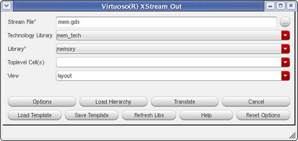
There may be some warnings, it's ok to ignore them here, but make sure to read the log file to get an idea about what the warnings are about.
Then you can close this pop-up.
Now you can find three files generated in the abstract directory. The .gds file is the binary GDSII file includes the layout information of your design library. xStrmOut_layerMap.txt is a layer map file describing how OA layer names and Stream layer numbers are mapped, and it will be needed when you import GDSII back to OA-based Cadence tools. strmOut.log is the log file for the stream out process.
1.3 Go through Abstract flow
The Abstract tool is the tool that takes your design and makes an “abstract” view of the design so that it can be used as a layout component. Conceptually this is like making a symbol for a schematic. But, it’s more complicated because you need a lot more information than just the pin names that you use in schematics. You need both symbolic and physical information and timing so that the place and route tools can incorporate your design into a larger layout successfully. The Abstract tool can use either the GDS file we created above and create the library component from that, or it can use the library itself to create a component. The first way is more flexible if you are importing a layout from some other source.
We show that first
1.3 Using GDS files
Now exit virtuoso, and start abstractor from Terminal:
> abstract &
Click File -> Library -> New...,
Fill in a new library name (e.g.
mem), click OK.
Then click File -> Library -> Attach Technology..., choose the new tech lib we created in virtuoso (e.g. mem_tech), and click OK.
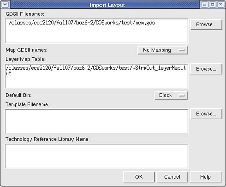
Next, click File -> Import -> Stream...
Find the GDS file and layer map table file generated by virtuoso,
change "Default Bin" to "Block", then click OK.
If by mistake the GDS is imported to the "Core" bin, you can then
select the cells and click Cells -> Move... to move them into the Block bin.
Don't extract your design in the Core
bin if it has multiple pins with the same name (or logically connected), but
these pins are not physically connected. For example, this may happen if your
have a large design with multiple power/ground rails running in parallel and
you name all of them VDD/GND.
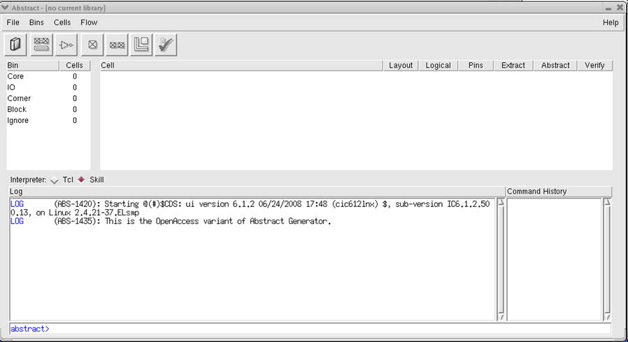
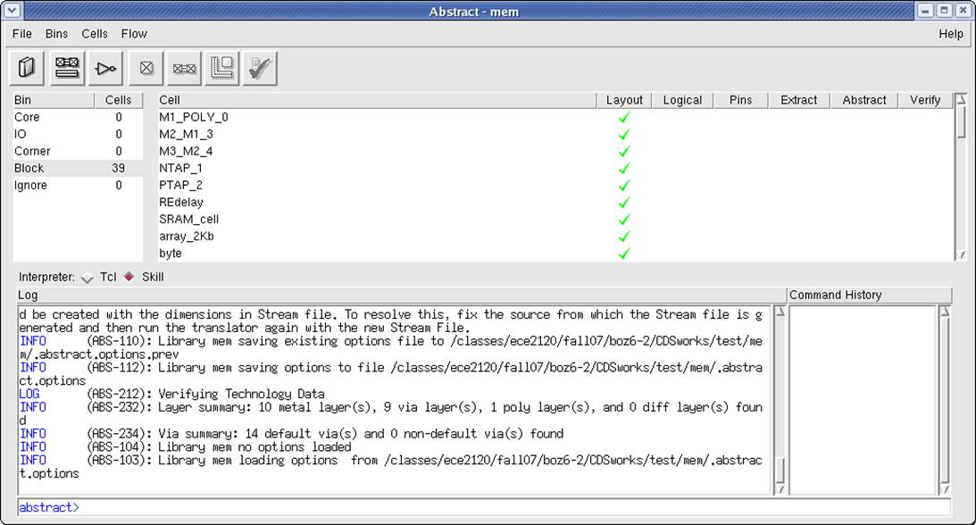
Now, the Abstract window should look like:
1.3 Using the Open Access (OA) files
Once you have your design in the library manager it is kept in the open access database. Therefore you do not need to write GDS and then re-import GDS to make a new library.
In the case above we made the library “mem” from the gds file. That library only had layout information, there were no other views. The first library we made: “memory” had all the layout and also all the schematics views. To use that library one can follow these steps:
Start abstract
> abstract &
Click File -> Library -> Open...,
In this way, when the abstract is created, it's automatically added to your cell as a view called "abstract", together with the existing layout, schematic, symbol, etc. Also note that in this way, when importing GDS file (next step), some other cells related to technology will be added to your design library and make it messy.
1.3 Back to generating the abstract view
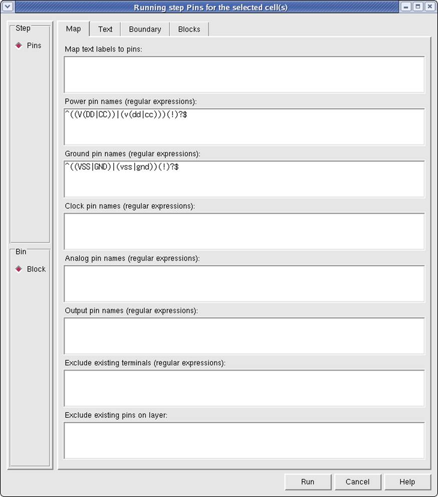
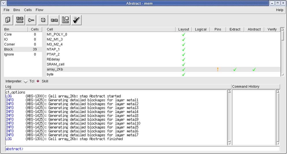
Click on the top level design you would like to extract (e.g. array_2Kb), then click Flow -> Pins... (or use the "Pins" button). In the pop-up window, click Run. This step is to extract the location, shape, size and layer information of the pins, and will create an "abstract.pin" view in the library.
This may result in some warnings in the log window; it's ok to ignore the warnings after you read them.
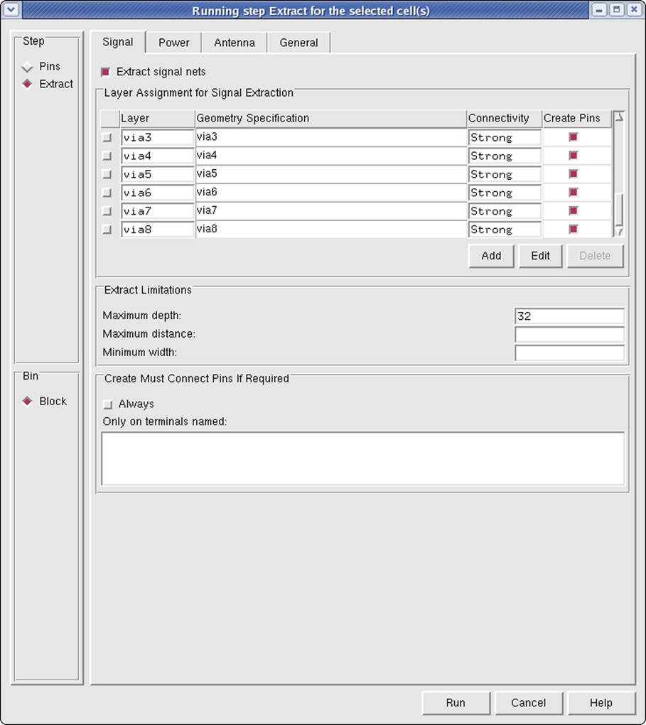
Then click Flow -> Extract... (or use the "Extract" button). In the Signal tab, enable "Extract signal nets"; in the Power tab, enable "Extract power nets". By enabling these two options, Abstract will extract the metals and vias that are directly connected to the signal/power pins, and consider them as EXTENSIONs of the pins. This provides the Place & Route tools with more flexibility: rather than routing to the tiny pin, connecting to any part of the pin extension will be a successful pin routing. However, if some of your pin extensions occupy too much area and are too complex in shape, Abstract will complain about that as an error and exit without finishing the extraction. For example, the VDD and GND in the top level array_2Kb module can not be fully extracted, so I disabled "Extract power nets". It's ok to not use these two options as the Place & Route tools are still able to route to the extracted pins, it is just harder for them.
Leave other options unchanged, click Run. This step will create an "abstract.ext" view in the library.
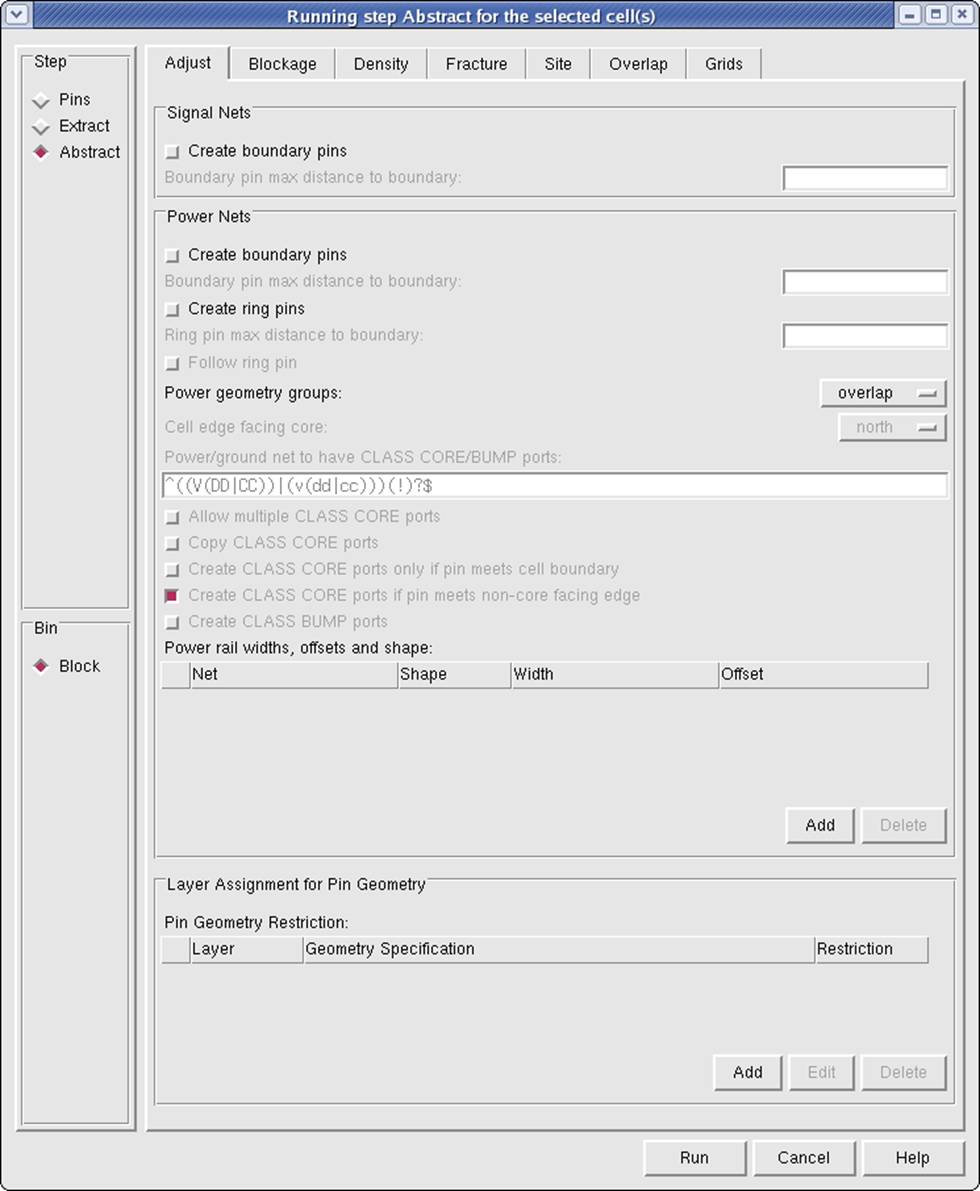
Then click Flow -> Abstract... (or use the "Abstract" button) In the Adjust tab, disable "Create boundary pins" for both signal nets and power nets. These two options would make routable pins at the boundary of the block, and make pin extensions inside the block invisible to P&R tools. This would make the memory area a complete “keep out” zone. By not checking these boxes you are telling the P&R tools that if they can find a way into/over the cell and then connect to the pins inside the cell.
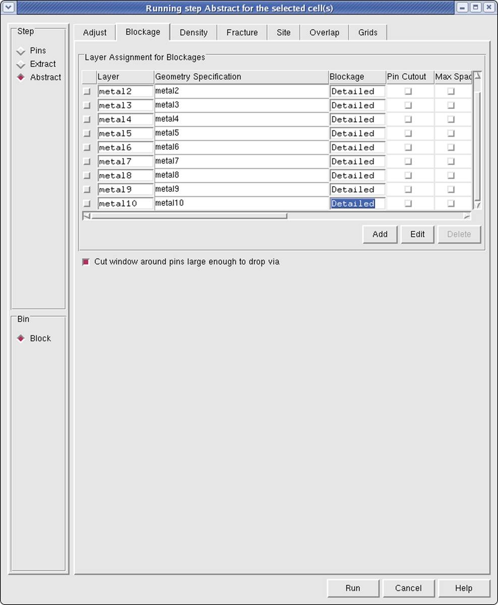
In the Blockage tab, change the
"Blockage" option of all layers from "Cover" to
"Detailed". Again, this says that the P&R tool should
actually look at the detailed metal layout to see how to route to the pins. Leave
other options as they are, click OK.
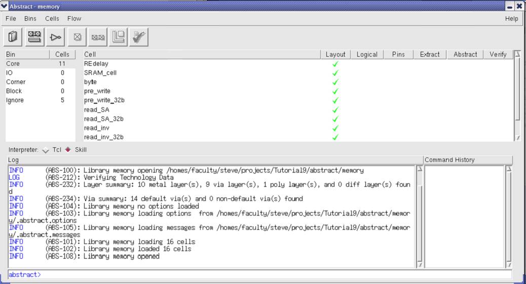
And now the Abstract window should look like:
As the verify step is optional (you can try it), we can now export LEF file. Click File -> Export -> LEF..., give the name of the LEF file, change "LEF Version" to 5.5, and make sure "Export Tech LEF Data" is disabled. Because our block was created and extracted with the same technology as the standard cell library, our LEF file is good enough to contain only the data of our custom block, as the tech LEF data is included in the LEF file of the cell library.
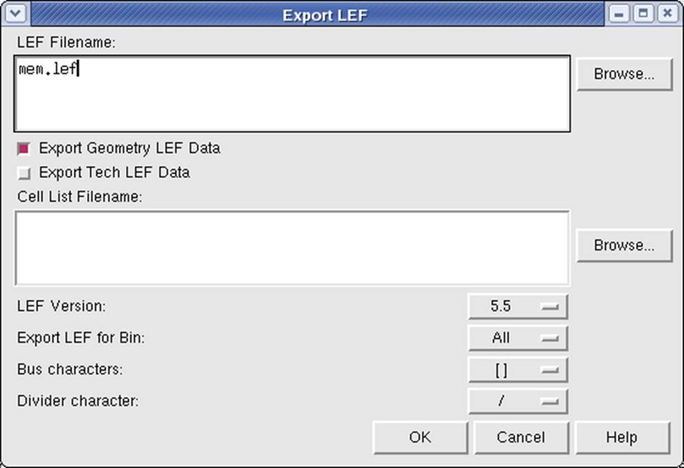
Now we get the LEF file for our custom block. It will be included together with the standard cell library LEF file when we use this block for Place & Route.
1.4 Alternative approaches
There is also an alternative, non-GDS-based method to get LEF file. The abstract generator tool is actually integrated with virtuoso. You can launch it in two places: 1) in the layout window of the design going to be extracted, click Tools -> Abstract Generation... 2) in CIW, click Tools -> Abstract Generator... It is pretty much the same as the standalone abstract generator, and you don't need to create a new tech lib as no GDS will be imported. After abstraction, in CIW click File -> Export -> LEF... to generate LEF file. The standalone abstract generator also works directly on your design library without a GDS file.
2. Preparing .lib, .db and Verilog files
During standard cell library creation, the cells are "calibrated" by EDA tools and the .lib and Verilog files are then converted from the calibration result. Cause our SRAM block is not possible to go through this procedure, I took one .lib file created by a memory compiler and modified block and signal names according to our block. The .lib file is then compiled into .db file using Library Compiler:
> lc_shell
lc_shell> read_lib array_2Kb.lib
lc_shell> write_lib array_2Kb
lc_shell> exit
As the function of this SRAM block is very typical, I hand-wrote a verilog file to describe its behavior. As the timing is already known from HSPICE simulation, I also added simple delay information of the read access to the verilog file.