Tutorial 7: More on Layout
This material is by Steven Levitan and Bo Zhao for the environment at the
University of Pittsburgh, 2008/2009.
Here are some notes for using the NCSU/OSU 45nm PDK
1. Generating Layout from
Schematics
1. If you are going to extract your layout, you must give all the pins
capital names when doing schematic and symbol, this is because the extractor
will generate all the pin names to be capital in extracted view.
2. Don't use poly pin, it will not pass LVS.
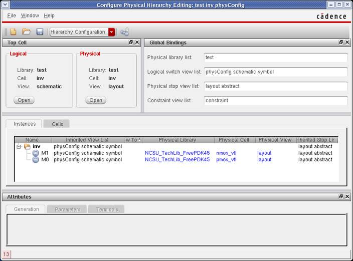
When configuring physical hierarchy, select
"NCSU_TechLib_FreePDK45" as Physical Library then find corresponding
cell as Physical Cell, as shown in figure 1.
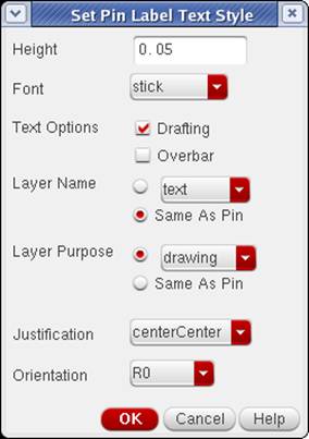
In "I/O Pins" section, select "metal1 dg" (other metal
layers will also work) as Default Layer, and click "Apply". Select
"Text Display" for "Pin Label Shape", then click "Pin Label Options...” Select "Same as Pin" for
"Layer Name", and change "Height" to 0.05, then click OK, as shown in figure 2.
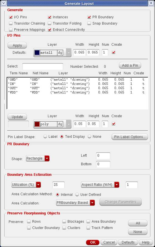
The "Generate Layout" window should finally look like figure 3.
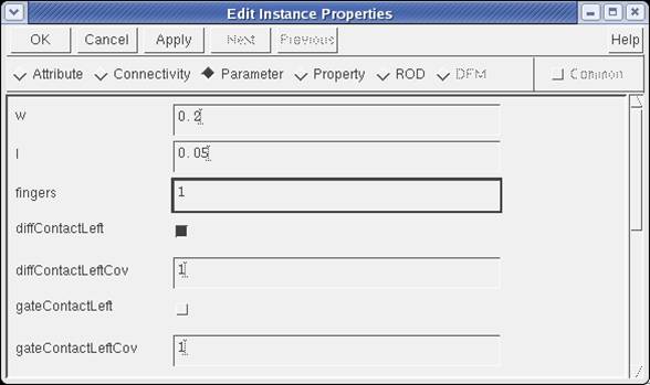
When transistors and pins are generated, you should find that the
transistors are not properly sized according to the schematic. Select one
transistor, click Q for its property, then select
"Parameter". Note that the sizes are labeled incorrectly in
"micro meter" in the layout, but are set correctly in
"meter" in the property. Change width and length into micro meter
values in property, as shown in figure 4, then click OK,
you should see the change in layout.
2. Running LVS
We are going to use Calibre for DRC, LVS and
extraction. For DRC, find the menu button "Calibre"
in the menu bar of layout window, click "Run DRC". In the DRC window,
everything is already set, but I highly recommend you to create a separate
directory for DRC, LVS and extraction, and set that as "Run
Directory" in "Rules", rather than using the current directory.
Otherwise, you are quite likely to be messed up by the many files generated
after DRC, LVS and extraction. Click "Run DRC", then you will get the
DRC result.
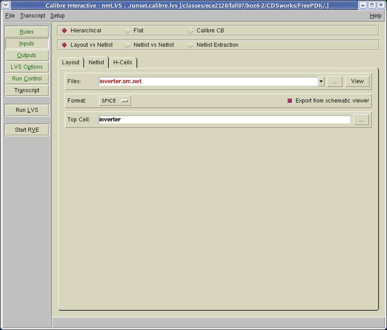
For LVS, click "Run LVS". In the "Netlist"
tab in "Input", select "Export from schematic viewer", as
shown in figure 5. Don't forget to change "Run Directory".
Click Setup -> LVS Options, in the "Connect" tab in "LVS
Options", select "Connect all nets by
name". Then click "Run LVS". Good luck.
If you get several LVS errors, don't try to solve them one by one. Browse
all of them and think about which one(s) may be most important. Because errors
may propagate, many errors will vanish when some "true" problems are
solved.
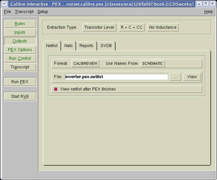
For extraction, click "Run PEX". In the "Netlist"
tab in "Input", select "Export from schematic viewer".
In the "Netlist" tab in
"Output", select "CALIBREVIEW" as Format, as shown in
figure 6.
Click Setup -> PEX Options, in the "Connect" tab in "LVS
Options", select "Connect all nets by
name". Then click "Run PEX".
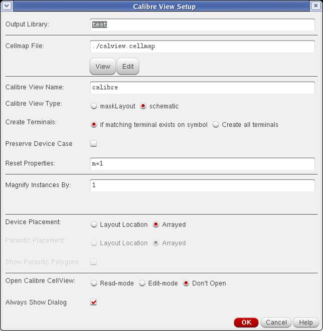
After a short while, the "Calibre View
Setup" window pops up. Select "schematic" for "Calibre View Type", and select "Arrayed" for
"Device Placement", as shown in figure 7. Leave other options
unchanged, click OK.
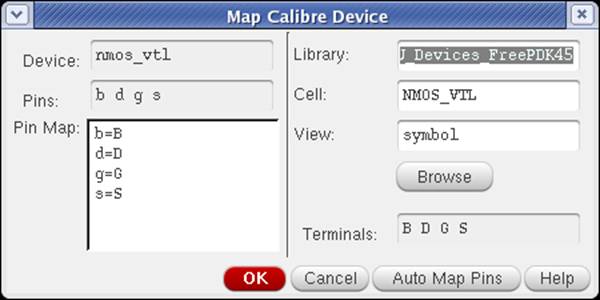
Then, you will have 4 "Map Calibre
Device" windows. The first two are for nMOS and pMOS, it should already found the cell view for you, so just
click "Auto Map Pins", make sure all the pins are mapped correctly
(two same characters with different cases are mapped), click OK, as shown in
figure 8.
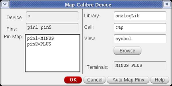
When the window for capacitance (c) pops up, replace the original Library
with "analogLib", then fill "cap"
into the Cell blank, it will find two Terminals MINUS and PLUS, click
"Auto Map Pins", and then OK, as shown in figure 9. For resistance,
fill "res" into the Cell blank.