Tutorial 4: Layout Generation and
Editing with Layout XL
This material is by Steven Levitan for the environment at the University
of Pittsburgh, Fall 2008.
We are using the NCSU 1.6 Beta CDK and Virtuoso 1.6.1.2
Please consult the
NCSU EDA Wiki
for background information
Many thanks to the team at NCSU for all their hard work!
Please see our
tutorial on setting up the design environment and running Virtuoso
Start with an Existing Schematic
- Start the Cadence Design Framework (virtuoso)
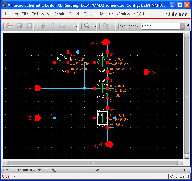
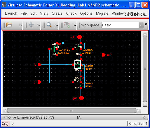
- Use virtuoso to create and simulate a 2 input NAND
gate schematic (called NAND2 in the library Lab1)
- Once you are happy with your simulation, close the ADE
simulation windows
Create a New Cell View
Open the library manager by selecting Tools->LibraryManager. This window allows you to browse the available libraries and create your own.
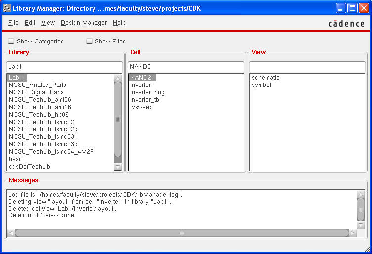
Create New Layout View
Next, select the NAND2 cell the Library Manager and select File->New->Cell View.... We will create a layout view of
the NAND2 cell. Simply NAND2 should be filled in for cell-name and change the
view to "layout" under view. Click OK or hit "Enter". Note that the "Application" is automatically set to "Layout
XL", the layout editor.
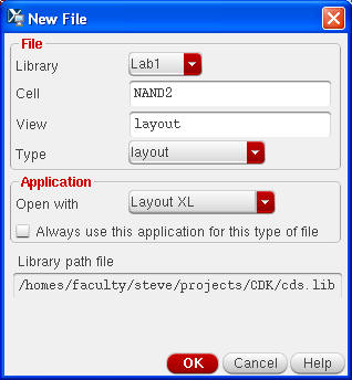
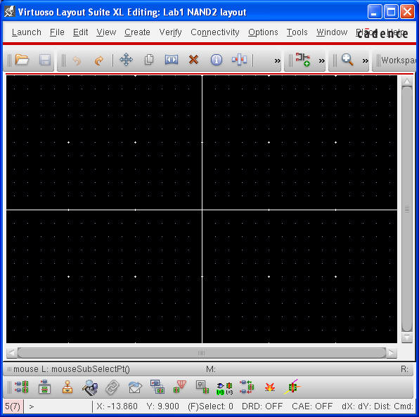
This will open two windows The first is the schematic window you just
closed, and the second is the layout window below
The layout window will be empty. NOTE unlike the schematic window, the
layout window does have and use coordinates for physical positions. You want
to build your layout at the origin to simplify the use of the cell by place
and route tools later.
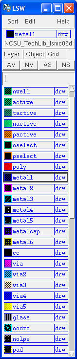
In addition, the LSW window (Layer Selection Window), which shows various
mask layers, will automatically pop up.
Configure Physical Hierarchy
For the CDK 1.6 beta TSMC02d library the physical names of the
transistors for layout and the logical names used in the schematic do not
match
Therefore the transistors need to be mapped. To do this go to the layout
window and click Launch->Configure
Physical Hierarchy
.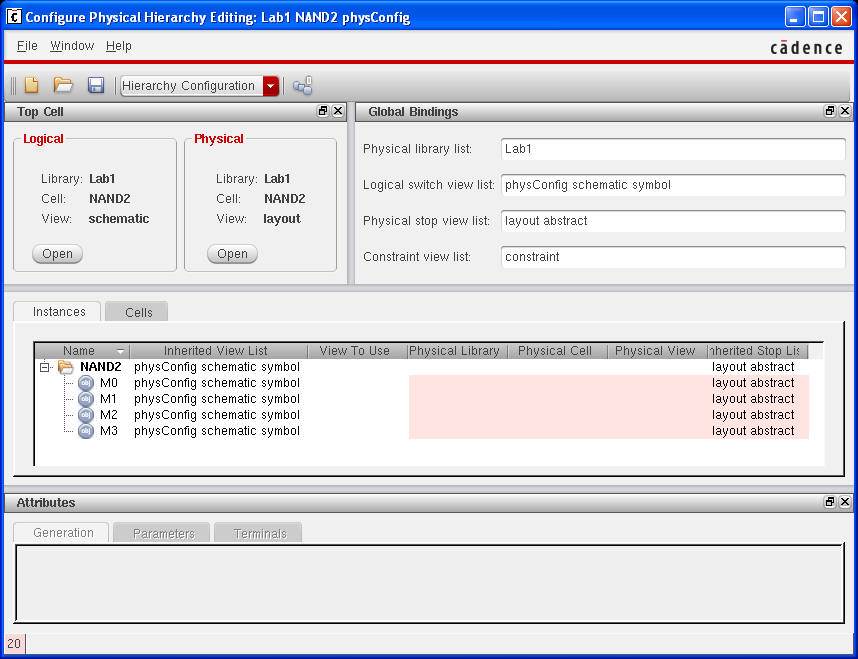
Now you must set the physical library and physical cell name for each
transistor. Double Left Click on the pink area under the words "Physical
Library" This will bring up a scroll menu for you to select NCSU_tsmc02d
then double left click under Physical Cell to select nmos (or pmos)
for each transitor NOTE there is no "4"
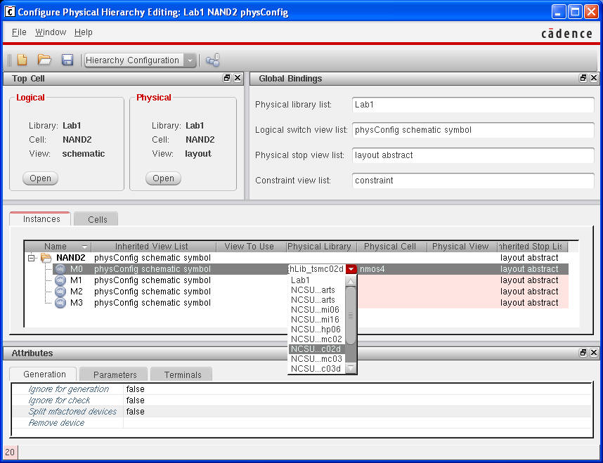
Once you have done that correctly, the line for that device will turn
blue:
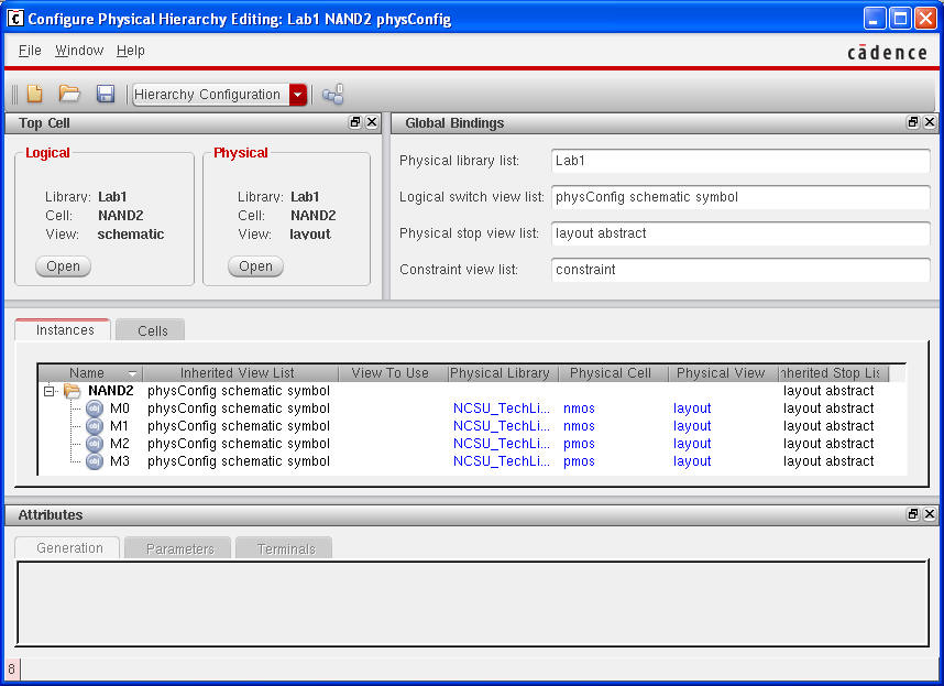
Save and close this window.
Create the Layout
You now have two choices. You can create (drag and drop) instances of
transistor "P-Cells" into your schematic "by hand", or you can let Virtuoso
XL find the cells in the schematic and put them in the layout for you. In
either case you must first perform the mapping of logical to physical cells.
The primary difference between Virtuoso L and XL is that XL attempts to
maintain the "layout vs schematic" (LVS) information from the beginning of
the process. That means it can directly generate the basic components into
the layout for you, and it maintains connectivity information between the
two views. This is not essential since we always verify that the layout is
correct using the LVS verification path as well.
Creating the Layout "by Generation"
Select
Connectivity->Generate->All from Source The following popup appears.
The defaults should be set for you, as below:
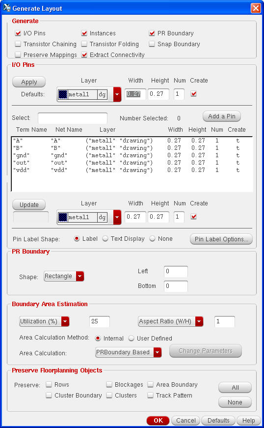
click OK
The layout should now look like this with all the correct
transistors/sizes and pins already put down for you:
Now you need to move the cells into position and wire them up. Note
that when you move the cells orange "flylines" will appear telling you
what should be connected to what, based on the connectivity in the
schematic. Also the pins for vdd, gnd, A and B have already been created.
Other than that, the process of wiring up the cell is pretty much the same
as below.
Creating the Layout "by Hand"
Now you are ready to draw objects in the Virtuoso window. In this section
you learn to place copies of other cells: pmos and nmos. These
cells are parameterized cells (or p-cells) which change their
features when you change their parameters.
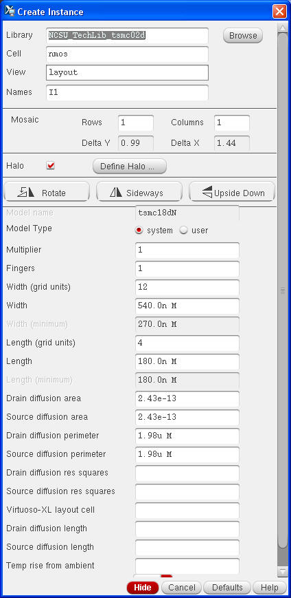
In Layout Editor select
Create->Instance, or simply hit "i". This will pull up the "Create
Instance" dialog box. Next, click "Browse" on the screen that appears and
select the library "NCSU_TechLib_tsmc02d", cell "nmos", view "layout". Click
"close" on the browser window. Then scroll down in the create-instance
dialog to look for a parameter called Width. Make sure this is set to
the same value as in you schematics (e.g., 540nm).
Next, move the cursor into the layout editor window. You should see a small
instance at the tip of your cursor, as shown below.
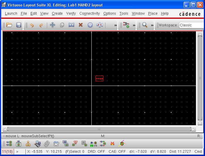
You may want to zoom in before placing the instance. To do that,
right-click and drag a box around the origin. When you
release the button, you should see that the instance is much larger.
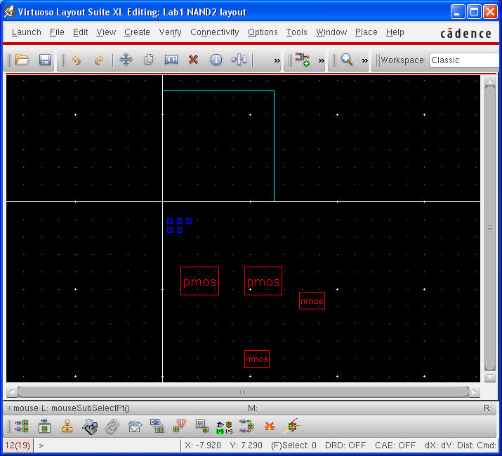
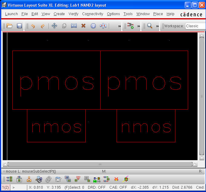
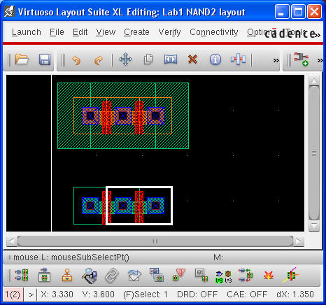
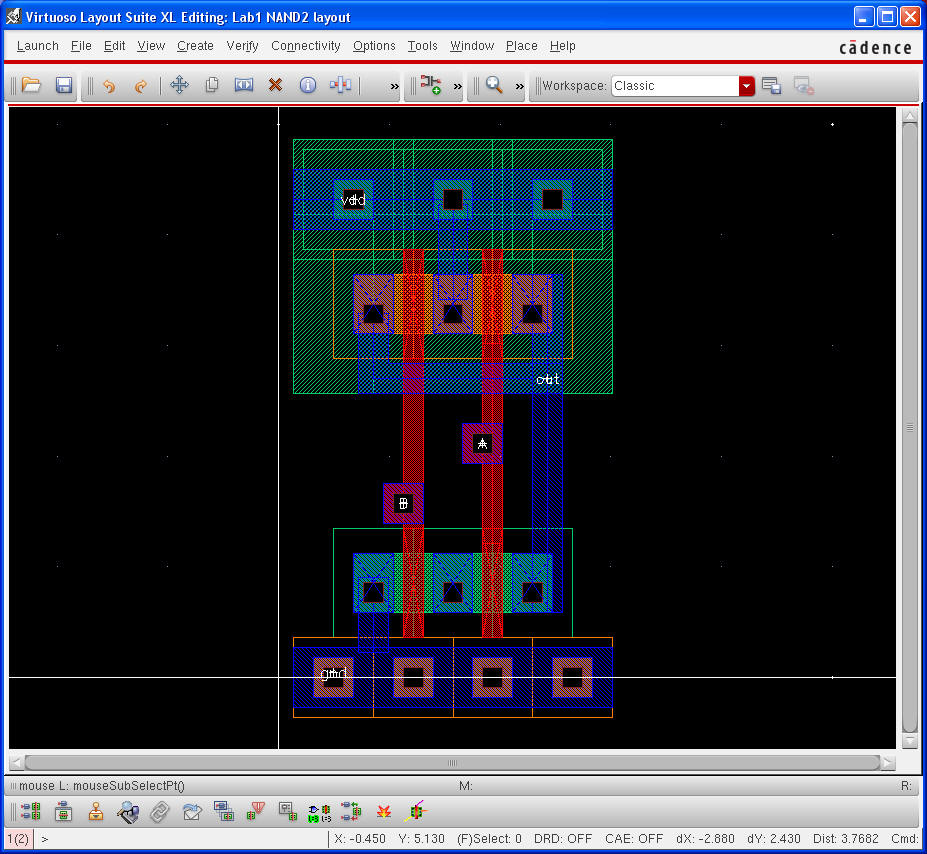
Place the two NMOS and two PMOS transistors so that your layout looks
like the window below. Finally, hit "Escape" to stop adding instances.
Now, you will notice that you don't immediately see what is inside the
nmos symbol. You can fix this by hitting Shift-F to display all levels
of hierarchy. (You can also do this by going to the Virtuoso Options
menu, choosing Display and setting Display Levels from 0 to
32) To switch back, hit CTRL-F, or set the Display Levels back to 0 from the
Options menu.
You may want to adjust your view so that it looks nicer. To zoom in,
right-click and drag a box around the area you want to zoom in.
Alternatively, you can hit "f" to "fit" the entire design in the window, or
SHIFT-Z and CTRL-Z to zoom in and out by factors of 2.
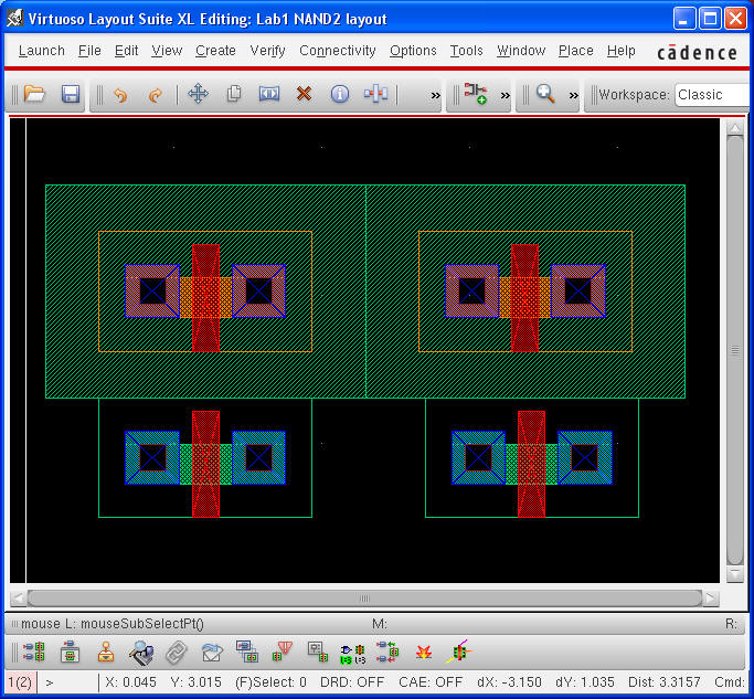
Use the commands above to show the layout as below.
Now, look now at the LSW (Layer selection window). This window shows you
the names of the layers that are "valid" (meaning that you can manipulate
them). You can figure out which layers are part of the NMOS cell by making
them visible and in-visible. To toggle a layer’s visibility, middle-click on
the name of the layer in the LSW. You can make all layers visible with the
"AV" button, and no layers visible with the "NV" button. F6 to "redraw" the
Virtuoso window after you’ve changed the visible layers.
Note that even if you make all layers invisible, you may still see some
shapes. This is because not all layers are "valid". Shapes in invalid layers
cannot be altered and are always visible. To make all layers valid, you can
choose Edit->Set Valid
Layers… in the LSW. In general, it is recommended that you not set
all layers as valid, because this clutters up the LSW with many unused
layers.
Using this approach, you should be able to figure out that the NMOS uses
the following layers: nactive, nselect, poly, metal1,
and cc (contact cut). The PMOS is like it, except that it uses layers
pselect and nwell instead of pwell and nimplant. Note that
there is nothing magical about the p-cells. You could paint these shapes
manually in the current cell-view, and it would make no difference
whatsoever to the tool. However, it’s much less effort to use the p-cells,
so that’s what we’ll do.
Note also the letters "drw", "net", and "pin" next to each entry
in the LSW. These are the purposes of a shape. The purpose is used to
indicate special functionality of a shape. We will discuss these more in
later tutorials. For now, remember that "drawing" is the purpose that
indicates that a shape will appear in the mask layout. You will sometimes
see "drawing" abbreviated as "drw", and sometimes "dg".
Selecting and Moving Layout
By default, if you simply drag out a region while holding down the left
mouse button (Button-1), whatever is within the box will be selected and
highlighted in white.
- Drag a box over the nmos you just instantiated. When you release the
mouse button, whatever is "selected", in this case the nmos cell, will
be highlighted.
Once you have selected an object (that is, an instance or a shape) you
can do lots of things with it.
- For example you can move it by typing the m hot-key. You can move
layout up/down/left/right one grid at a time by clicking at the
selection and moving the mouse. Try it.
You can also select objects by clicking on them.
- Clicking the left mouse button once on an instance or shape selects
it.
If you didn’t place your NMOS and PMOS cells exactly as illustrated
above, try moving them now until they are.
DRC
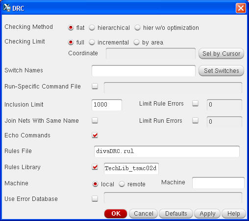
To perform a Design Rule Check (DRC), choose
Verify->DRC….
The DRC form appears, as shown below. Then click "OK". If you do not see the
window appear, or if you get an error, then it's possible that you didn't set up your environment in the correct order.
For this technology we will use the "DIVA" DRC and extractor tools. These are
part of virtuoso and should be set up correctly for you.
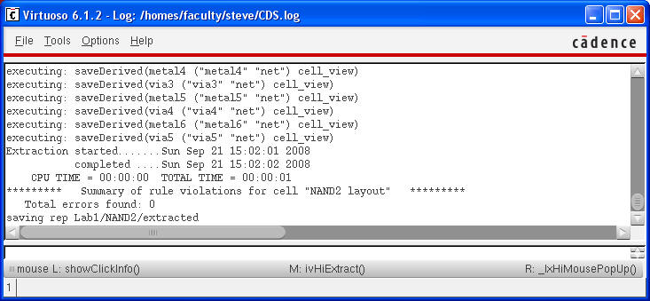
You will see a bunch of text scrolling through the log window. NOTE,
even though most of the information in the log window is boring, it
often has key information about what Virtuoso is doing, so it is very useful
to keep this window open and read the messages there.
Viewing DRC Errors
After running DRC the layout window shows the DRC errors as white
polygons:
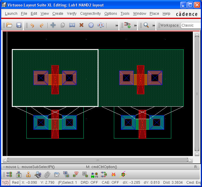
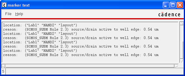
You can learn about the errors by clicking on the
Verify->Markers->Explain
This shows the text explaining the error in a pop-up window
Choose Verify
->Markers->Find ...,
select "Zoom to Markers and click "Apply" and then Next. The screen should
zoom to the error and the explain error box should show you the
corresponding error. NOTE: The DRC errors are keyed to the
"official" DRC design rules for the process. In our case, these match with
the explanations in our text book, and on the MOSIS pages for this process.
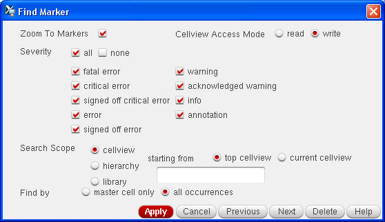
You can delete all markers with
Verify
->Markers->Delete All
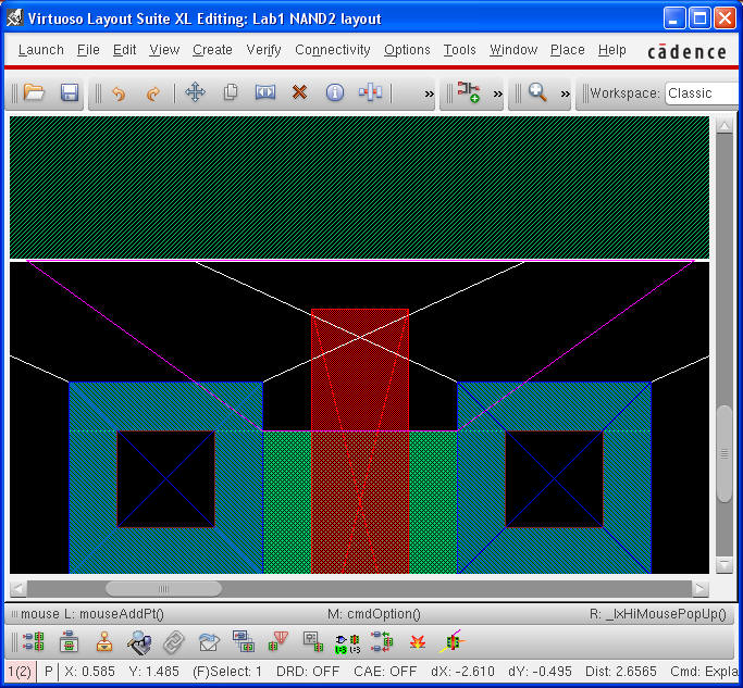
In this particular case, the transistor wells are too close together. Fix this error by moving up the pmos. It’s good practice to space the NMOS and PMOS transistors by the smallest amount allowed in order to make the layout as dense as possible.
Later on you will see that we do not always want to put them as close as
possible. You can draw temporary rulers by hitting "k" and dragging a ruler. You can clear the rulers by hitting "Shift-K". These rulers can help you to draw dense layout much faster than you would by constantly running DRC.
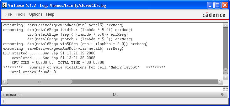
Move the PMOS and re-verify until there are no DRC errors
Using some of the XL features
Open the schematic window. Now with both windows open, click on the
transistors in the schematic window. Similarly, if you click on the
transistors in the layout window the transistors in the schematic will be
highlighted. As we add nets and net names, more correspondences will be
tracked.
Now move the PMOS and NMOS transistors so that they share common contacts
as shown electrically in the schematic. We have put the upper nmos
transistor to the right of the lower one, this is because we will be taking
the output of the gate from the right side of the layout.
Painting, Wiring, Segments, and Paths
Before we get started wiring up the schematic note that we are really
just creating the fabrication masks for the creation of the final chip. This
means, among other things, that it usually does not matter how you create
the shapes in the layout, and it usually does not matter if the
shapes of the same material overlap - creating "redundant material." In
the end it will be the final geometry that gets exported (via the "GDS"
output file) to make the masks to make the chip.
So, you will see some tutorials use "painting rectangles" while others
use "wiring tools" and others use "path editing tools" all to achieve the
same ends. There are advantages to each, but they all work.
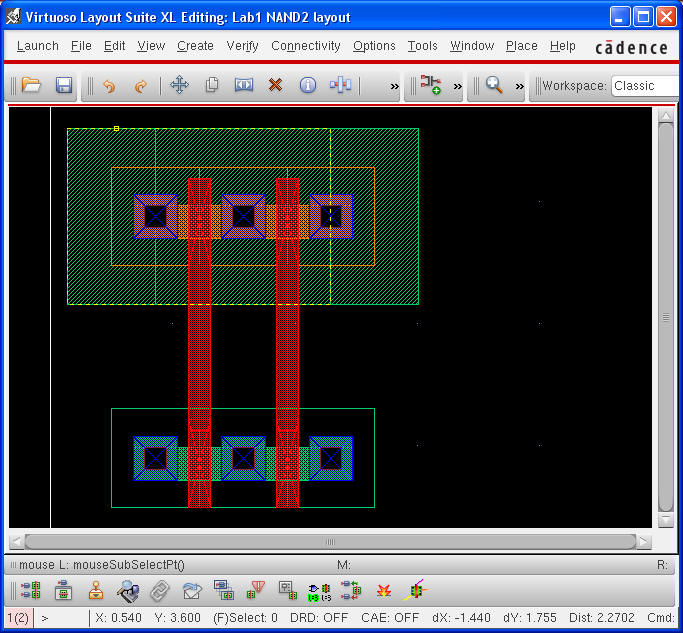
We are now going to "paint" a piece of poly to connect the pmos and nmos devices together. We do this by creating a shape, in this case, a rectangle.
- Select the poly layer in the LSW by left-clicking on it.
- Use Create
->Shape->Rectangle Or
hit “r” to draw a rectangle and draw the poly area.
- Hit “Escape” to stop drawing rectangles.
- Your layout should look like this:
You can do the same thing with the PATH command. The path command is a
little different in that it knows what the minimum size for each layer is,
and gives you a way to draw in that minimum size. Also you can add bends
with the tool. Finally, paths can be stretched more ways than rectangles.
- Use Create
->Shape->Path Or hit “p”
to draw a path and draw the poly area.
- Double click the mouse without moving it to stop that path
- Hit “Escape” to stop drawing paths.
If you don’t like the way your drawing turned out, you can select a shape and delete it with the delete key, or you can hit “s” (for stretch), and click on one of the sides of a path or rectangle to stretch it into the position that you like.
Now select metal 1 on the LSW pallet and then create a path for the
output of the circuit. Note the contacts for each transistor already have
metal1 as part of the contact structure.
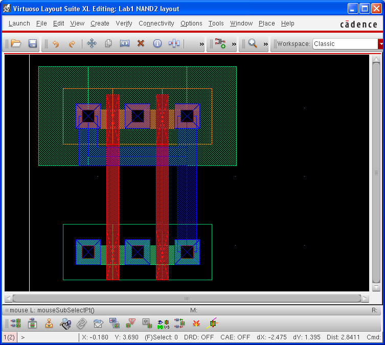
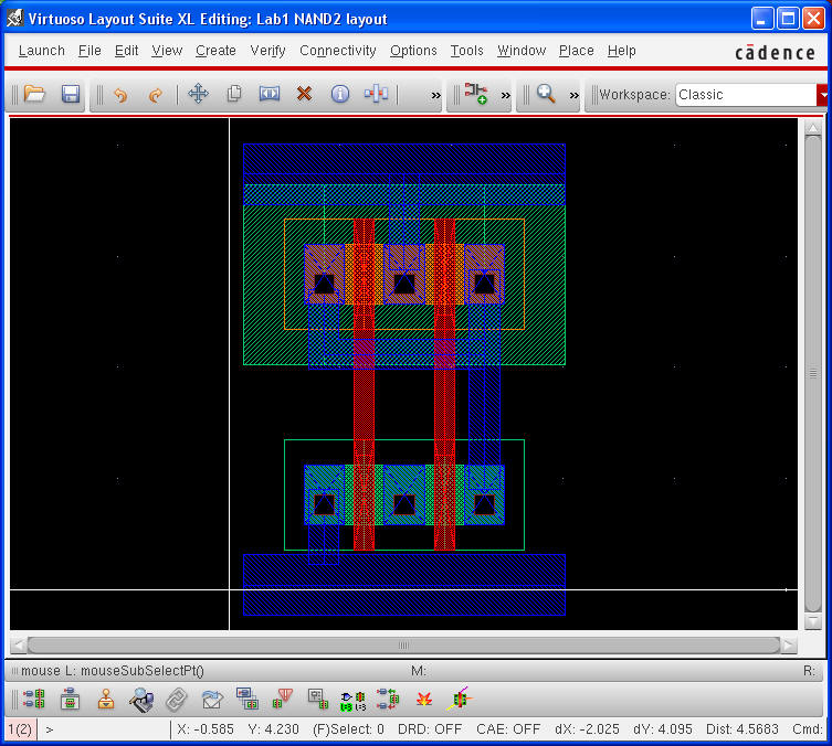
Next, create strips of metal1 for VDD and GND. We typically make these shapes as horizontal bars across the top and bottom, and therefore call them “supply rails”. We then need to connect the rails to the source nodes of the transistors. Create these rails now, and make your design look like the one below. Again, try to make the layout as compact as possible
but make the supply rails double the minimum width for metal1, running DRC as often as needed to learn the design rules.
If you get confused about which transistor is which, use the XL
schematics window to see what should be connected to what. NOTE in
this figure I also changed the transistor sizes from 270nm to 540 nm to
match the schematic. This can be done by opening the object properties
pop-up.
Add Vias
Next, we need to add contacts to wells, which serve as the bulk node of the transistors.
NOTE "Via" is a general term for connections vertically between
layers. Typically people use the words Via and Contact Cut interchangeably. But
really, the contact cut is just the "black hole" between layers and the Vias are
the composite structure of the contact cut, and the two rings (one in each
connecting layer) around the contact cut.
Transistors do not have well-contacts by default, because they take up so much room. Several transistors can often share the same well-contact.
In this class, we will require that every gate (that is, NOT, AND, OR, XOR, etc.) has at least one contact to each well
or the substrate.
Create an NTAP via by choosing Create->Via... You should see the Create Contact pop-up appears, as shown below. Set the "Via Definition" to "NTAP". The other options should be set
correctly by default. Place it as close as possible to the PMOS transistor.
I like to add multiple Vias, they take up no more space, in this case and
they give lower resistance to the well.
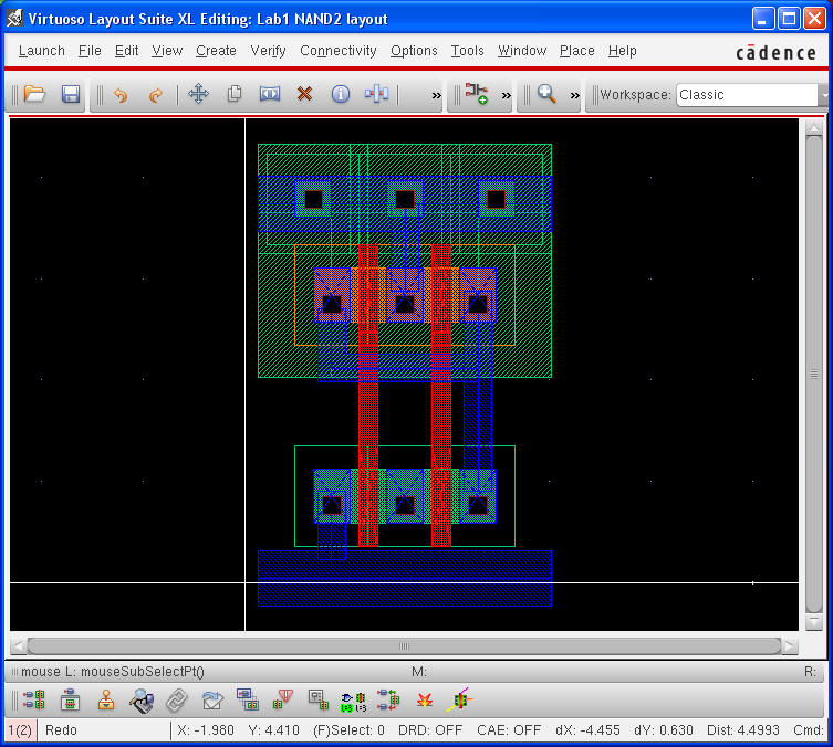
For this process, we do no have a PWELL we only have P-Substrate. None
the less. we need to bias the nmos transistor body to ground. Unfortunately
we do not have a PTAP cell so we just use a contact to P-Active
(M1-P) and place it as close as possible to the NMOS transistor. Again, try to make the layout as dense as possible. We will need to connect these NTAP and PTAP cells to the power rails. Create metal1 rectangles to connect these contacts to the rails. When you are done, your layout should look approximately like the one below.
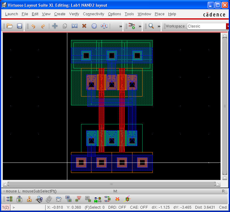
Next, add a two gate-connection in metal1, with a metal1-to-poly via. Do this by choosing Create->Via... again and set the contact type to M1_POLY.
Position the vias over the poly lines as shown below
NOTE
in order to fit both poly
contacts we had to move the output line to the right, and we had to move
both the PMOS transistors and all the wiring up. The stretch command is very
useful for these operations. It is important that there be a way to wire the
inputs and outputs to other cells in metal.
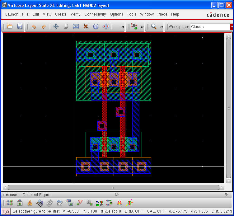
Create Pins
Lastly, we need to create pins so that the nodes in our layout have names that are human-readable. Create these pins by selecting Create->Pin…. You should see a dialog box appear, like the one below. Type the names vdd!, gnd!, in, and out in the “Terminal Names” text-box as shown below. Select “Display Pin Name”. Leave all other options as they are.
Next, click the “Display Pin Name Option…” button. You will see another dialog box appear:
Set the height to 0.090 um and the layer to metal1-dg (drawing). Click OK.
Next, click on the layout where you want each pin to be placed. You will need to click three times: twice to create a rectangle for the pin, and a third time to place the label. The shape of your rectangle doesn’t really matter, as long as it only covers area that is already covered by metal1-dg. When you are done, your layout should look like the one below.
Note now, with layout XL you should be able to click on NETS
as well as the transistors and verify the connectivity in the layout.
Congratulations! You have completed the tutorial. Save your design and select
File->Export image
and use a white background, to print out a copy of your layout.
Extraction
Now use Verify->Extract
to extract the cell. Set swich to Extract_parasitic_caps. This will
create a new view in the cell library called the "extracted view" This will
be a netlist (like a spice netlist) but generated by virtuoso examining the
layout and identifying all the components and nodes it finds.
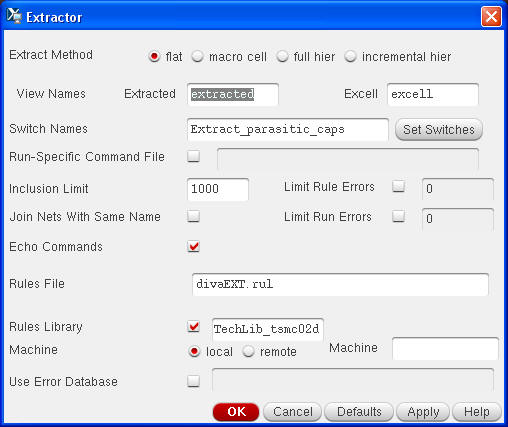
NOTE Do not open the Extracted view at this time (its fine later) but
the next step (LVS) does not work if the extracted view is open, even though
we use the extracted view to perform LVS
Layout vs. Schematic (LVS)
Use Verify->LVS
to bring up the LVS pop-up. Make sure you "use data from form" and set the
form to use the schematic and extracted views these might not
be the default.
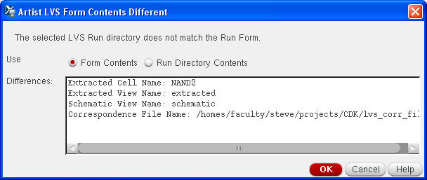
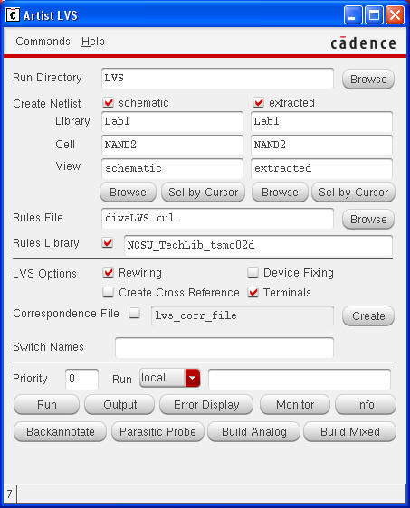
Click Run in
the LVS window. It might ask you about saving cell views - say yes. LVS
takes some time, watch its progress in the log window.
If things are set up correctly you will get a popup like this:
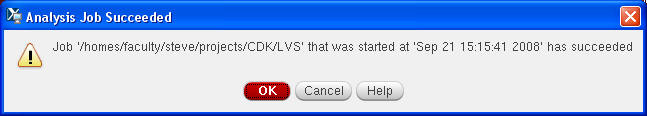
NOTE the LVS job succeeding DOES NOT mean that the layout
and schematic match. It just means the job ran (like a SPICE run). You need
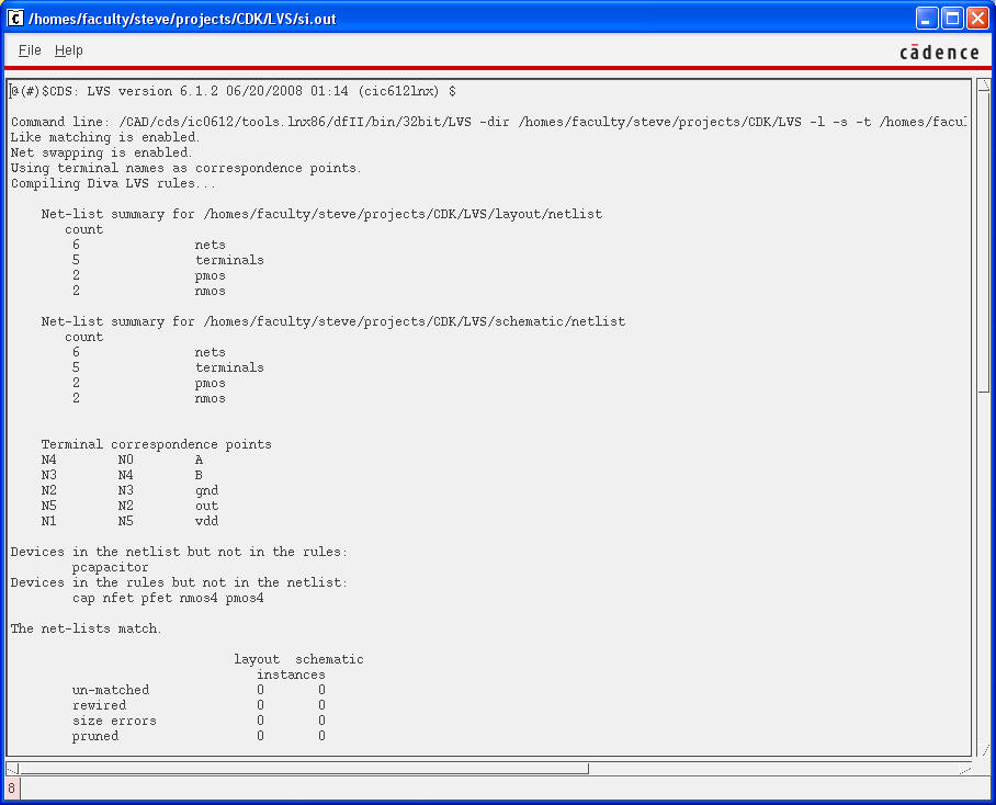
to look at the output to see if it really matched. If they do, then the
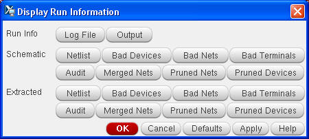
output will show that the netlists match. If not use the "info" button to
bring up a menu of files to look at to help figure out what went wrong.
If not use the "info" button to bring up a menu of files to look at
to help figure out what went wrong.
Simulating the Extracted Layout
Now, go to the TEST BENCH that you (should have) made for your original
schematic. We got fancy here and made a custom symbol for the NAND gate, but
its not important what shape it is. The advantage of having a separate test
bench cell (nand_tb) is that we can re-use this test bench for all our two
input gates.
We can also use the same test bench to compare our schematic simulation
with a simulation of our extracted layout.
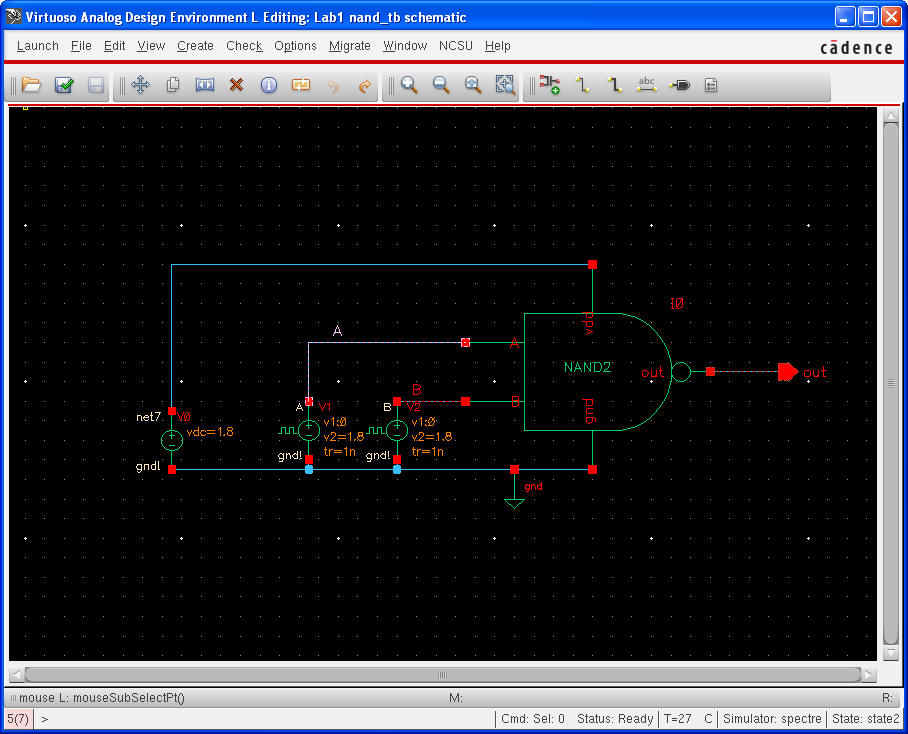
Start Analog Design Environment from the test bench schematic. Run your
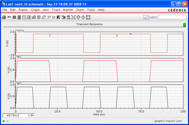
test of the NAND gate schematic. You should get something like this:
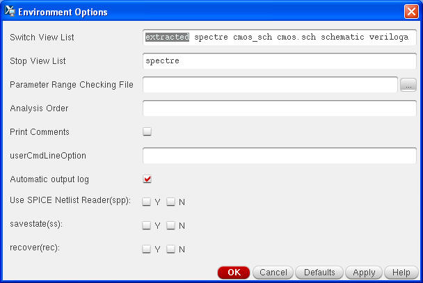
Then use Setup->Environment to
bring up the pop-up below. Add the word "extracted" to the switch view list.
This list is the order of cell-views that are searched when ADE is looking
for the sub-circuit NAND2 for generating the netlist for simulation. By
putting "extracted" before "schematic" in the list, you are saying you want
to use that view (if it exists).
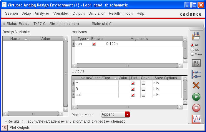
ALSO change the plotting mode from "replace" to "append" Now run (or
re-run) the simulation
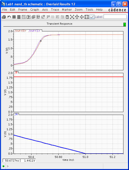
The simulation waveform should show you 3 more waves, appended to the
bottom of the previous trace. You can delete the second copy of A and B
since the signal generators are the same. You can now overlay the two copies
of the "out" trace. They should look almost identical, but if you zoom in
you should see that the extracted design is just a little slower due to the
parasitic capacitances you extracted.
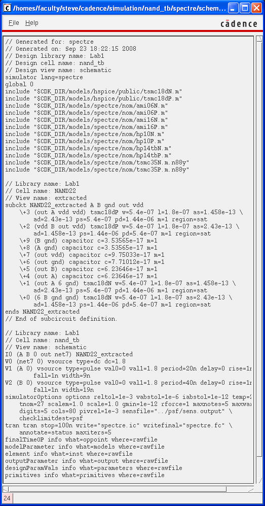
Look at the Netlist
If you look at the netlist generated by ADE (Simulation->Netlist->Display)
you can see two things, one that the sub-circuit is from the extracted view,
and two that there are very small capacitors that now appear in the netlist.
Further Reading
If you would like to learn more about the layout editor, you view the Cadence documentation. Start the documentation browser by typing
cdsdoc &
at the command prompt, make sure that IC6.1.1 is selected in the Active Library pull-down box at the top, and then select Virtuoso Layout Editor->Virtuoso Layout Suite L User Guide in the browser window that appears. This should start an HTML browser that displays the table of contents for the tutorial.