Tutorial 10: Utilizing Custom
Block for Synthesis, Place & Route
This material is by Steven Levitan and Bo Zhao for the environment at the
University of Pittsburgh, 2008/2009.
·
Updated
24-Feb-2010 by Bo Zhao
We are using the NCSU/OSU FreePDK, Synopsys Design Compiler, Encounter 7.1, and Virtuoso 1.6.1.2
Please consult the NCSU EDA Wiki for background information
Many thanks to the team at NCSU and Oklahoma State University
Please see our tutorial on setting up the design environment and running Virtuoso
Before you get started, you should understand that these tools are very powerful and have lots of options. What we are showing here is one simple path through the design flow. To understand the tools, and their power, you must explore their capabilities by reading the help manuals, and trying lots of tests. Use the configuration files and scripts to keep your work manageable, and keep notes about what works, and what does not, so you don't make the same mistakes over and over.
Please read / do Tutorial 9 before you do this tutorial. Here we assume you have already built and abstracted a design for a custom sub-component.
In Tutorial 9 we created a custom SRAM array ready for use
with synthesis and place & route tools. This tutorial will show how to
include this block in your design and go through the flow.
Depending on how you generated your custom block (top down
or bottom up) you might need to (re)integrate your custom block with the rest of
your design at the HDL level, or just at the schematic /layout level. The first
part of this tutorial assumes you build the Memory “bottom up” and now have to
integrate it into your HDL design.
1. Synthesis
In your HDL design file, simply utilize
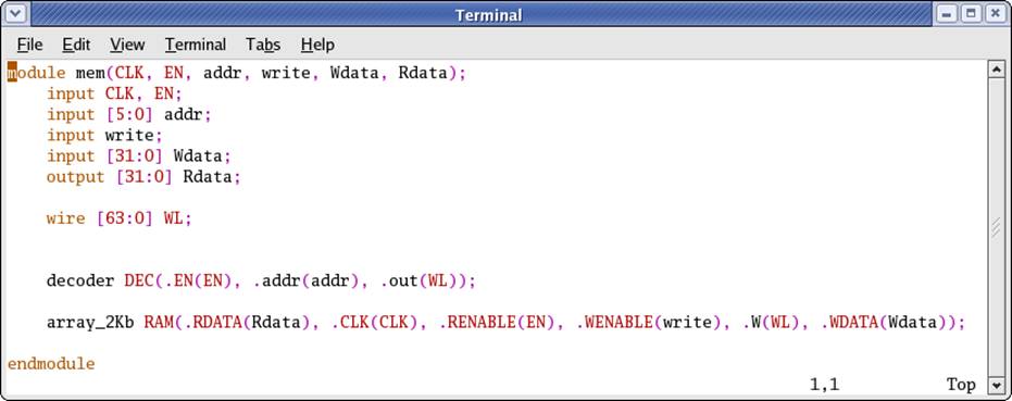
"array_2Kb" as a component, which has the following interface:
input CLK; //originally called PRECHARGE
input
RENABLE; //read enable
input [63:0]
W; //64 wordlines, comes from the output of decoder
input
WENABLE; //write enable
input [31:0]
WDATA; //32 bits of write data
output [31:0]
RDATA; //32 bits of read data
Note that this block "array_2Kb" does not contain
a row decoder, and we can build one for it out of standard cells. Please find
$CLASS/lib/mem_lib/mem.v as an example. This file
utilized array_2Kb as a component and accompanied it with a row decoder. So it
is actually a small complete SRAM block with all necessary peripheral circuits.
It is very important that a decoder is required
whenever/wherever you use array_2Kb as a component. As mem.v
already did this, you can actually always employ this file in your design
instead of always writing your own row decoder. Although it's in Verilog, it will be effortless for you to rewrite it into
VHDL.
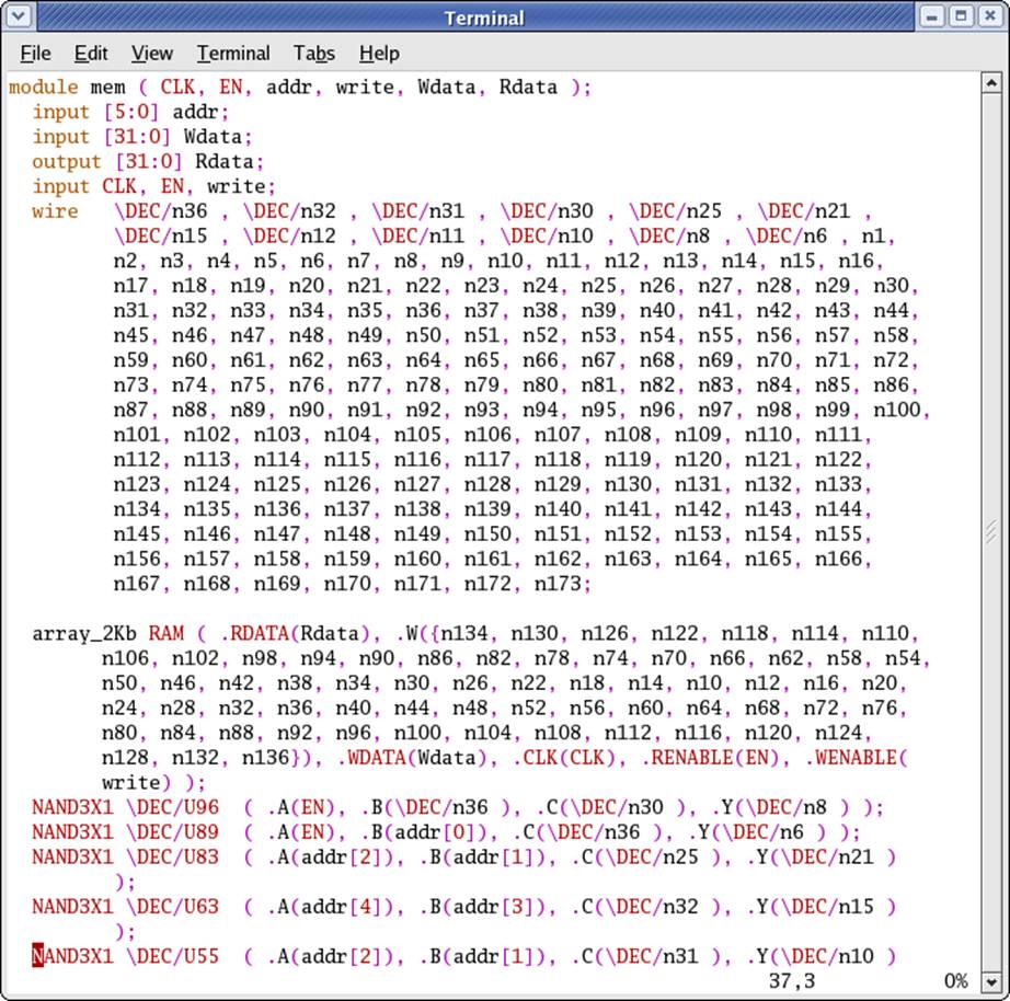
Then you can synthesize your design as usual. After
synthesis, you will find the "array_2Kb" is still synthesized as a
component reference, while other circuits are in standard-cell format.
For post-synthesis simulation, both gscl45nm.v (contains all
standard cells) and array_2Kb.v (contains SRAM block) should be compiled prior
to your synthesized netlist.
We then use the netlist mem_SYN.v synthesized from mem.v
for place & route.
2. Place & Route
The basic procedure is still the same as standard-cell-only
P&R, so I listed the main differences here. Please use the following
comments as a complement to the instructions in the earlier P&R tutorials.
All these comments are relative to the steps in the flow discussed there.
NOTE: Besides the
following comments, you should really play around with Encounter for various
kinds of settings and options to find the "sweet spots" that make
your design happy.
2.1 When importing design
Make sure
array_2Kb.lib is in "Common Timing Libraries", together with the
original file "gscl45nm_new.lib".
Make sure
array_2Kb.lef is in "LEF Files", together with the original file
"gscl45nm.lef".
These should
already been filled if you load the configuration file $CLASS/flow/place_route/OSU.conf
2.2 After importing design
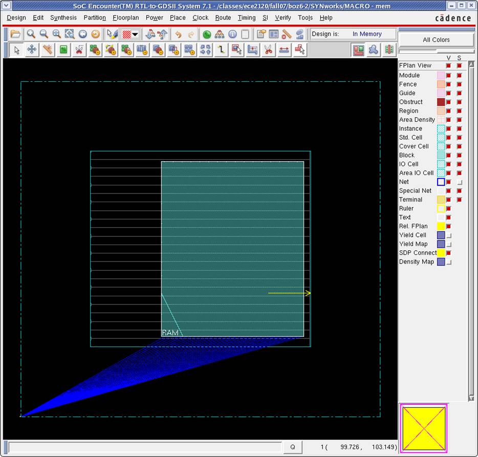
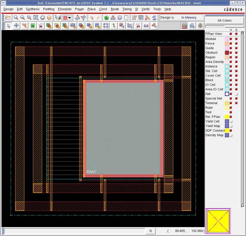
You will find a green/blue box placed next to the core area
(the "multi-row" rectangle), this is the SRAM block. After
specifying the floorplan, click the "move"
button (cross icon) in the tool bar, then click the
block, move you mouse to move it to your preferred location inside the core
area.
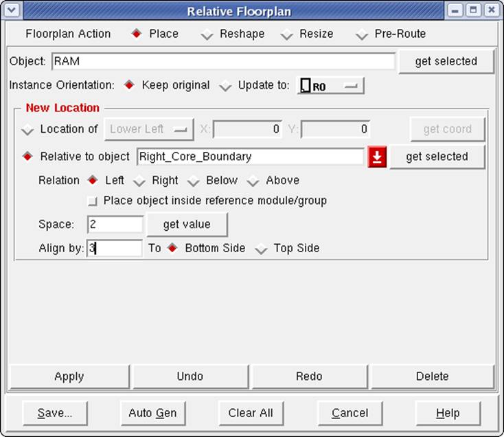
For more precise control, you can align block(s) relative to some references. Click Floorplan -> Relative Floorplan -> Edit Constraint..., then you can specify how the block is placed. For example, the following setting tells Encounter to place the block "RAM" on the left side of the right core boundary with spacing of 2um, and also 3um above from bottom side.
You can place blocks relative to boundaries, and also other
blocks. So if your design contains multiple such SRAM blocks to form a large
memory, you can easily align them into a matrix. It will be extremely useful to
extract the command of these settings from .cmd files
and write your own script to place a matrix of blocks by aligning the first one
to some boundary and aligning the rest one by one.
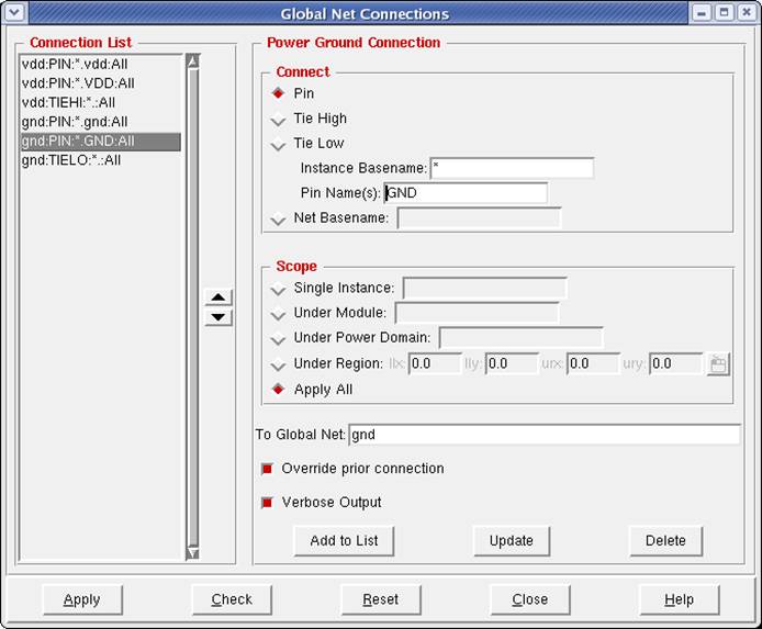
2.3 When connecting global nets
Add two connections for pin VDD and GND (we already have vdd and gnd), since the names of
power and ground pins of the SRAM block are in upper case.
2.4 After connecting global nets
Floorplan
-> Edit Floorplan -> Edit Halo
...
For "Placement Halo", fill in the halo width at
the four sides, then click OK. This will
generate a halo around the block in which no standard cells can be placed;
hence the halo width defines the minimum distance from this block to any
standard cell.
Floorplan
-> Edit Floorplan -> Set Block Placement Status ...
Click the SRAM block to select it,
select "fixed" as "Set to status", click
OK.
2.5 After adding power rings
Power -> Power Planning -> Add
Rings... (the same window you just used for
power rings around the core area)
Select "Block ring(s) around"
instead of "Core ring(s) contouring" for "Ring Type", set
the Width and Spacing for "Ring Configuration". You can
also use the graph in Advanced tab to build the Block
Ring.
A Block Ring needs to be built as a special power plan
since, compared to the standard cells, a block is not in the same size and its
power pins are not placed in the same style (in one word, it's not standard).
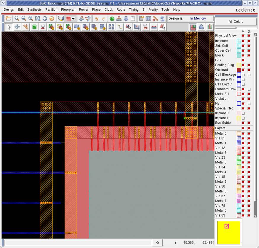
2.6 When adding stripes
In Advanced tab, select "Omit
stripes inside block rings" and "Omit strips over selected
blocks/domains"
It should now look
like:

2.7 When special routing
Enable
"Block pins" "Standard cell pins" and "Stripes
(unconnected)", keep disabling "Pad
pins" and "Pad rings".
Advanced -> Extension Control
Here we should
make sure the power routing for standard cells are not going through the block.
The following setting may not work.
select
"Nearest ring/strip" for second column (Block pins and stripe),
select "First ring/strip outside of row" for first colume (Standard cell pins). In the lower part, select the
second one "First stripe after the last cell". When you have problem,
please try different options to figure out which one is you want.
It should now look
like:
Note that the
power and ground pins of the block are all routed to the block rings.
After the rest of steps (fillers not placed), it should look
like:
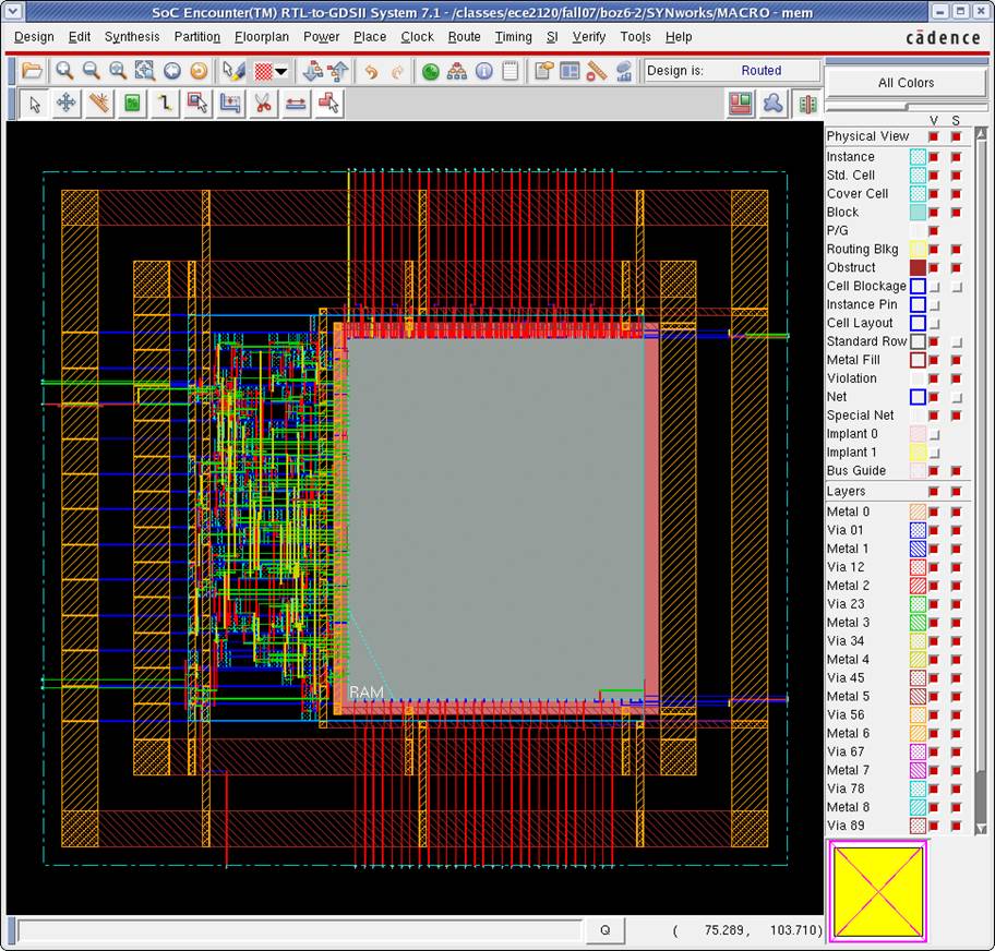
This is exactly what we expected: the SRAM array lies on the right and the row decoder on the left, address comes into decoders from left, and the decoder outputs (wordlines) are feeded into SRAM array to the right. Write data are parallely feeded in from top like a bus, and read data come out from bottom.