Tutorial: Virtuoso 6.1.2 Analog Artist with Spectre and the 1.6 (beta) CDK from NCSU
This material is taken from the NCSU EDA Wiki tutorial and has been modified by Steven Levitan and Bo Zhao for the environment at the University of Pittsburgh, Fall 2008.
Many thanks to the team at NCSU for all their hard work!
This tutorial will introduce you to the Cadence Environment: specifically Composer, Analog Artist and the Results Browser.
The screen-shots in this tutorial may vary slightly from what you will see. Refer to the text next to the screen-shot for up-to-date information. Note also that some screen-shots have been shrunk to make the page more readable. In this case, please click on the image to view its wiki-page, and click on the image again to download the full-size image.
Create Aliases to Setup Your Environment (only do once)
- Before you start this tutorial, add the following lines to the
.cshrc file in your home directory:
source /classes/ece1192/fall08/CLASS/dot_cshrc
You only have to do this one time, it will stay between login
sessions.
Start the Cadence Design Framework
- Log in to a Linux machine. The setup for this tutorial is currently supported only on Linux machines.
- Create a directory to run this tutorial, called something like "projects" (for cadence projects). Change to this directory.
- Type "setup_all" at the command prompt. This will add the tools to your search path, and run tool specific scripts for each of the tools in our environment.
- Start the Cadence Design Framework by typing "virtuoso &" at the command prompt.
[steve@SB1 ~]$ cd projects
[steve@SB1 projects]$ setup_all
You should see:
Cad set up as CAD_DIR = /CAD
Cadence set up as CDSHOME = /CAD/cds//ic0612
Hspice set up as HSPICE_ROOT = /CAD/synopsys/hspice/hspice
Ciranova is set up as CNI_ROOT = /CAD/ciranova/santana
NCSU CDK set up as CDK_DIR = /CAD/ncsu/install_dir/ncsu-cdk-1.6.0.beta/
[steve@SB1 projects]$ virtuoso &
The first window that appears is called the CIW (Command Interpreter Window).
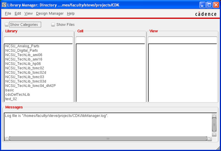
Another window that is very handy is the Library Manager, which allows you to browse the available libraries and create your own.
This window should come up automatically. But, if it does not, to display this window, choose Tools -> Library Manager... from the CIW Menu.
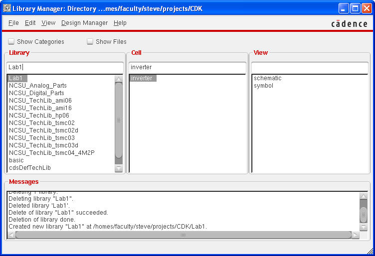
Create the Lab1 Library
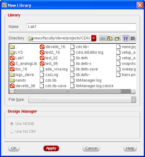
In the Library Manager, create new library called Lab1.
- Select File->New->Library. This will open new dialog window, in which you need to enter the name and directory for your library.
By default, the library will be created in the current directory. After you fill out the form, it should look something like this:
- Click OK.
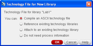
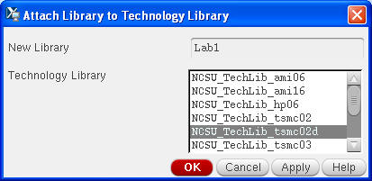
Next, you will see a window asking you what technology you would like to attach to this library.
- Select "Attach to an existing technology library" and click OK. In the next window, select "NCSU_TechLib_tsmc02d".
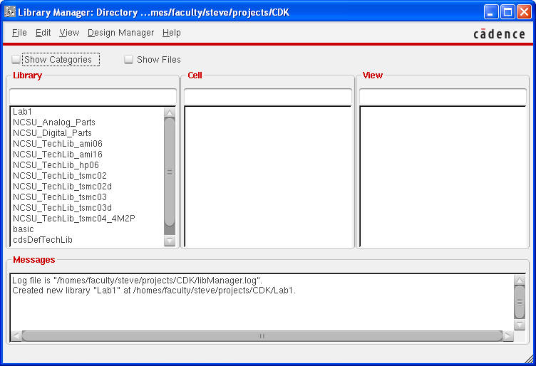
You should see the library "Lab1" appear in the Library Manager.
Create the Inverter Schematic
- Next, select the library you just created in the Library Manager and select File->New->Cell View....
We will create a schematic view of an inverter cell.
- Simply type in "inverter" under cell-name and "schematic" under view. Click OK or hit "Enter".
Note that the "Application" is automatically set to "Schematics L", the schematic editor.
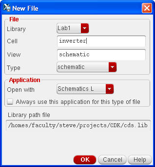
Alternatively, you can select the "Schematics L" tool, instead of typing out the view name. This will automatically set the view name to "schematic".
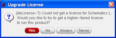
- Click Ok. You may see a warning about getting a license. the following window. Simply click Ok to ignore this warning or always to never see it again.
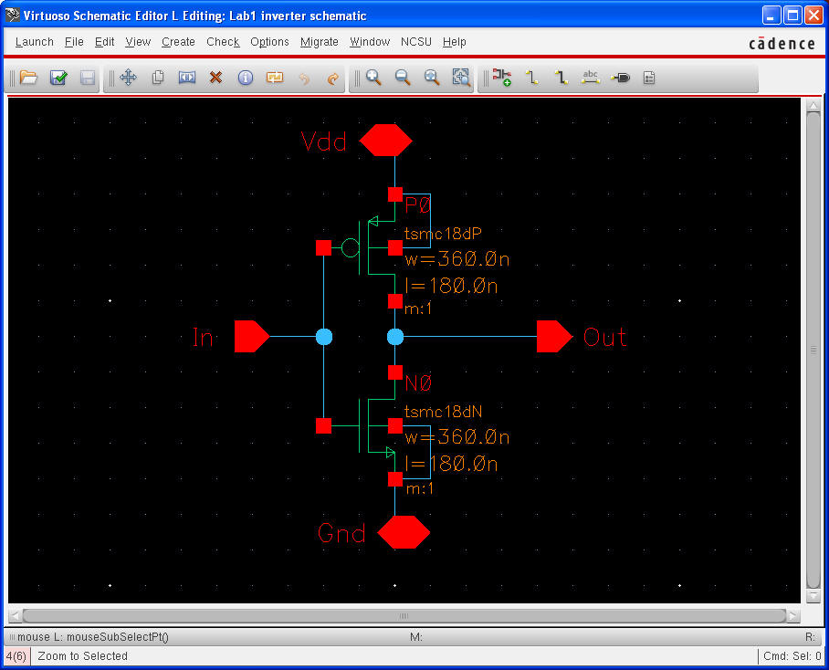
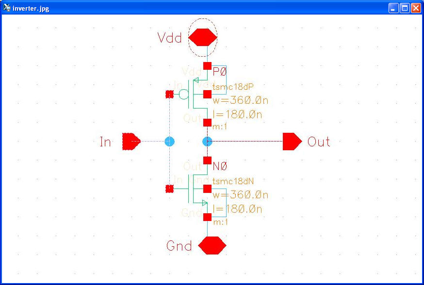
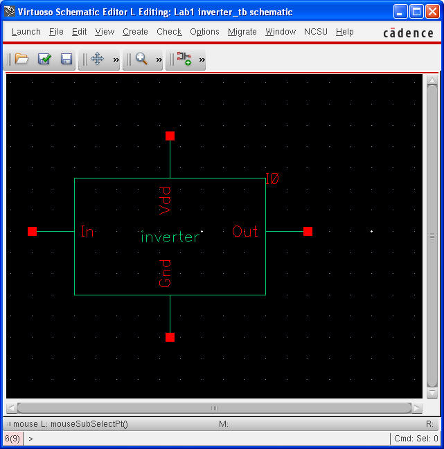
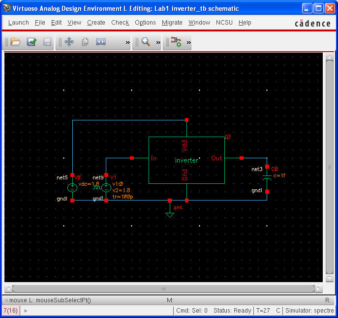
After you hit "OK", the blank Composer screen will appear. The image below shows the inverter schematic that we will make in this tutorial.

To generate a schematic like this, you will need to go through the following steps:
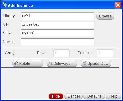
- From the Schematic Window, choose Create->Instance.... The Add Instance, dialog will appear.
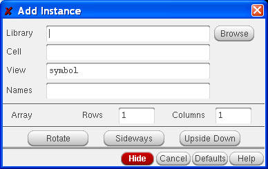
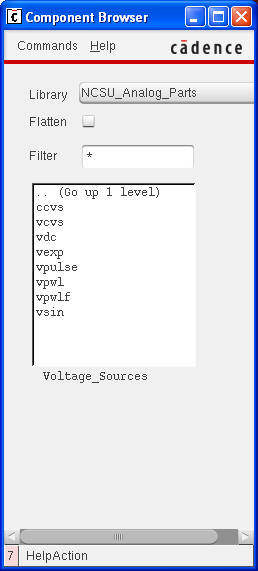
- In the Library field, select NCSU_Analog_Parts or Browse to the NCSU_Analog_Parts in the Library Manager
We will place the following instances in the Schematic Window from the NCSU_Analog_Parts library as instructed below:
Description Library Sub-directory Cell View NMOS Transistor NCSU_Analog_Parts N_Transistors nmos4 symbol PMOS Transistor NCSU_Analog_Parts P_Transistors pmos4 symbol Supply Nets NCSU_Analog_Parts Supply_Nets vdd, gnd symbol Voltage_Sources NCSU_Analog_Parts Voltage_Sources vdc, vpulse symbol Passive Elements NCSU_Analog_Parts R_L_C cap symbol
NOTE: pay special attention to the parameters specified in vdc, vpulse, and cap. These parameters are very important in simulation.
ALSO Note: use the nmos4 and pmos4 transistors, these have the body contact explicitly drawn, which will help later the design process.
Place PMOS Instance
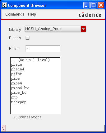
- In the Add Instance window, select the pmos4 cell from the library NCSU_Analog_Parts/P_Transistors.
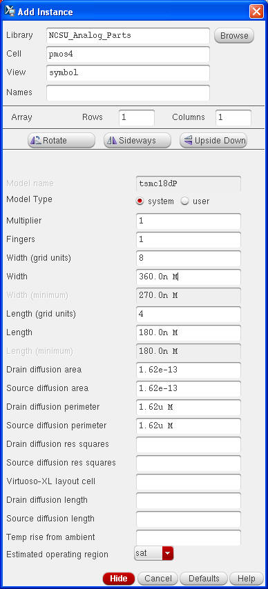
You may either type the values in or click Browse and find them in the Library Manager. After you select the cell, the "Add Instance" dialog will change to show the options for this cell. Set the Width to "360n" and the Length to "180n". Note that "M," for meters will be filled in automatically. Place the PMOS cell in the Schematic Window
Place NMOS Instance
- Next, in the Add Instance window, select the nmos4 cell from the library. Set the Width to "360n" and the Length to "180n". Place the cell in the Schematic Window. Your schematic should look like this:
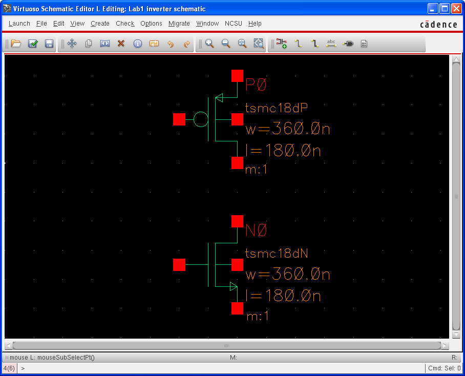
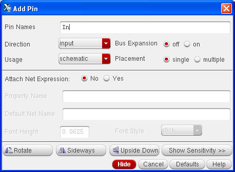
Place Pins
- Next, in the use Create->Pin command to add Vdd, Gnd In and Out pins. Use a input pin for the input, an output pin for the output and InputOutput pins for Vdd and Gnd
Place wires
- In the Schematic Window menu, select Create -> Wire (narrow)
- Place the wire to connect all the instances
Save the design
- Select File -> Check and Save.
Look at the CIW. You should see a message that says:
Extracting "Inverter schematic"
Schematic check completed with no errors.
"Lab1 Inverter schematic" saved
If you do have some errors or warnings, the CIW will give a short explanation of what those errors are. Errors will also be marked on the schematic with a yellow or white box. Errors must be fixed for your circuit to simulate properly. When you find a warning, it is up to you to decide if you should fix it or not. The most common warnings occur when there is a floating node or when there are wires that cross but are not connected. Just be sure that you know what effect each of these warning will have on your circuit when you simulate.
Your schematic should look like the one shown below.
Printing the Schematic
- Select File->Export Image. Fill in the name of the file you want to save to, and change the Appearance to be Solid and choose white for the background color.
Do not print or turn in schematics with black backgrounds - they use up too much printer toner and are hard to read.
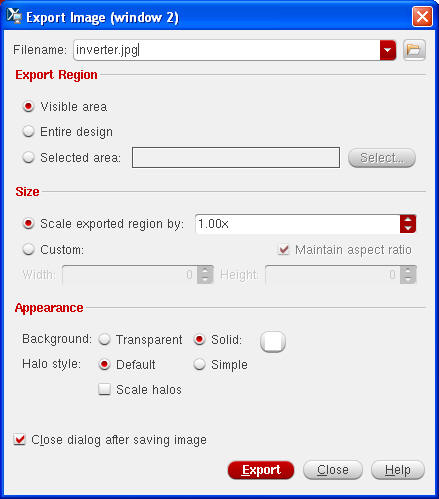
The saved JPEG image will look like this:
Create a Symbol for the Inverter
To keep a clean "design hierarchy" we want to separate the testing of the circuit from the circuit itself. One way to do this is by making a new schematic called a test-bench which will have the signal sources that will drive the circuit to be tested. This seems like extra work now, but it will turn out to be well spent as our designs get bigger and we have multiple views of each design.
- Select Create -> Cellview -> From Cellview.
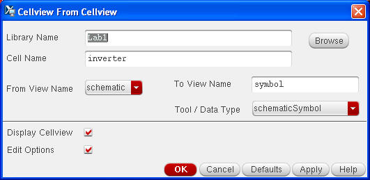
- Just say "ok."
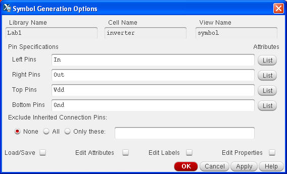
- In the symbol generation menu, place the pins on the top, bottom, left and right as you like:
- Click "ok" and a new schematic like window pops up:
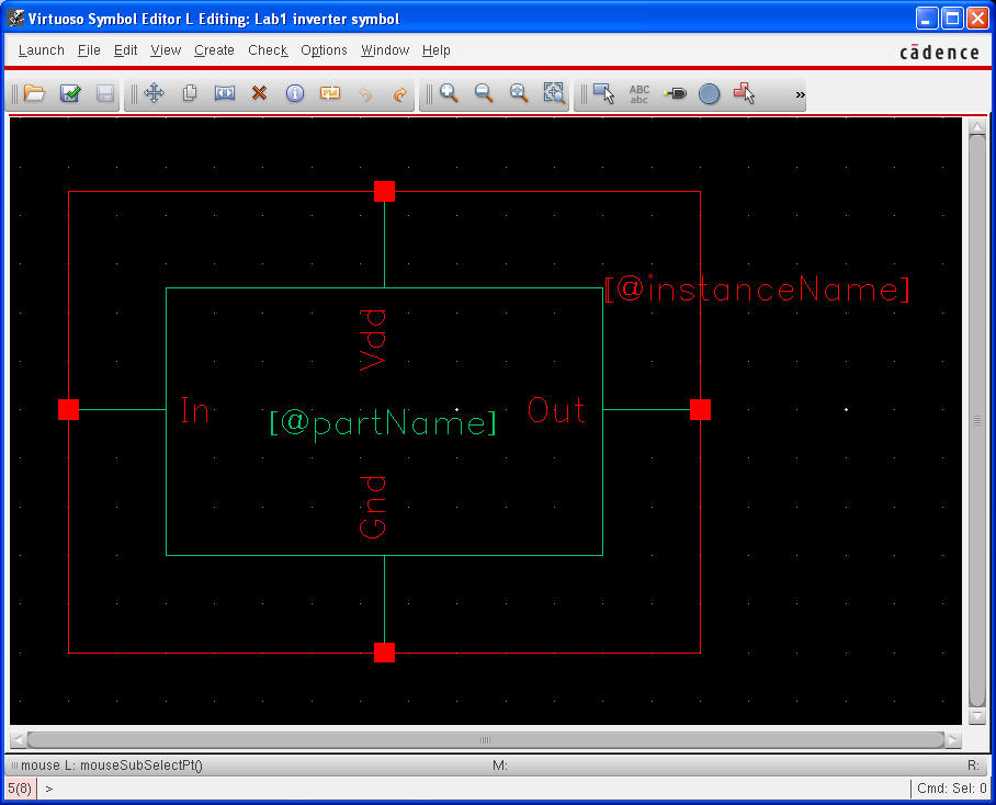
You pretty much never want to edit this symbol view of the inverter. You should just regenerate it, if you need to.
- Close this schematic and close the inverter schematic as well.
Create a Test Bench Schematic
Go back to the library manager, you should now see both the schematic view and the symbol view for the inverter.
- You should now add a new cell view to the Lab1 library, called inveter_tb for the test bench

In this new schematic we will put an instance of the inverter symbol as well as the test circuits.
Place the inverter in the test bench
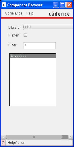
- Use the component browser to select the inverter symbol to place in the inverter_tb schematic.
- Place an instance of the inverter component in the inverter_tb schematic
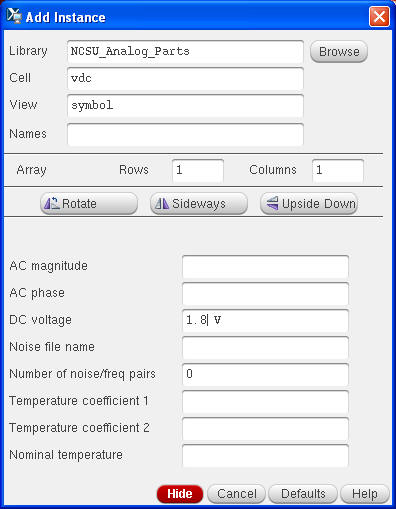
Place vdc Instance
- Next, from the NCSU_Analog_Parts Voltage Sources library, select vdc symbol. In the DC voltage field, enter 1.8 Note that the "V" will be inserted automatically. Place it in the Schematic Window.
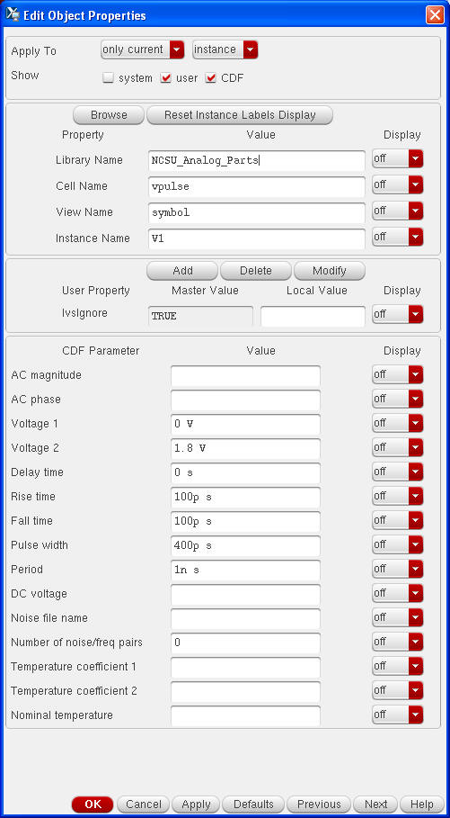
Place vpulse Instance
- Next, from the NCSU_Analog_Parts Voltage Sources library, select vpulse symbol. Enter the following values in the form and place it in the Schematic Window.
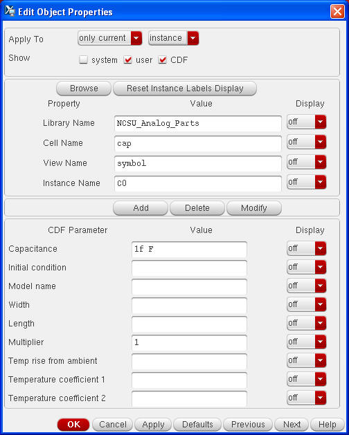
Place cap Instance
- Next, from the NCSU_Analog_Parts R_L_C library, select cap symbol. Enter "1f" in the Capacitance field. Note that the "F" will be filled in automatically. This will give us a 1 femto farad load capacitor. Place the instance in the Schematic Window.
Wire Up the Test Bench
- Use thin wires to wire the inverter to the sources and capacitor,
Add Ground Reference
- Also add the gnd symbol from the NCSU_Analog_Parts Supply_Nets library.
NOTE: this is very important! All versions of SPICE are very temperamental about needing a ground reference for simulation.
-
Save this design!
Keep the window open for simulation
For more Information about Virtuoso
If you would like to learn more about the schematic editor, you can work through chapters 1-5 of the Virtuoso Schematic Editor Tutorial that comes with the Cadence documentation. Start the documentation browser by typing
cdnshelp &
at the command prompt, make sure that IC6.1.1 is selected in the Active Library pull-down box at the top, and then select Virtuoso Schematic Editor->Virtuoso Schematic Editor Tutorial in the browser window that appears. This should start an HTML browser that displays the table of contents for the tutorial. You may also find the Virtuoso Schematic Editor L User Guide very helpful to describe some of the further commands available in the schematic editor.
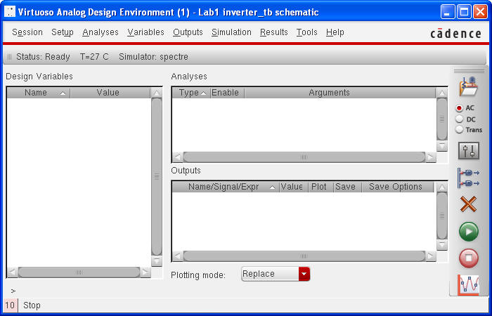
Simulate the Schematic with Spectre within Analog Artist
Set up the Simulation Environment
You are now prepared to simulate your circuit.
- From the Schematic Window menu, select Launch -> ADE L. You may get another message saying that the license need to be upgraded. Simply click Ok to proceed. A window will pop-up. This window is the Analog Design Environment Window.
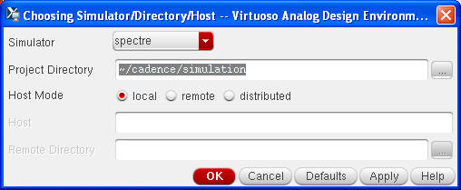
Choose a Simulator
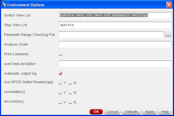
By default for our class the Spectre simulator is chosen. If you want to change it, from the Analog Artist menu, select Setup -> Simulator/Directory/Host. Enter the fields as shown below. Your simulation will run in the specified Project Directory. You may choose any valid pathname and filename that you like. Cadence generates many temporary files for simulation, so you do not want to leave them in your home directory.
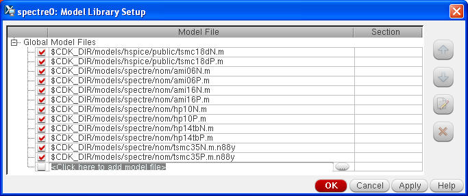
Setup for Simulation
Next, use the other setup menus to verify the settings for model libraries and simulation environment, these should look like:
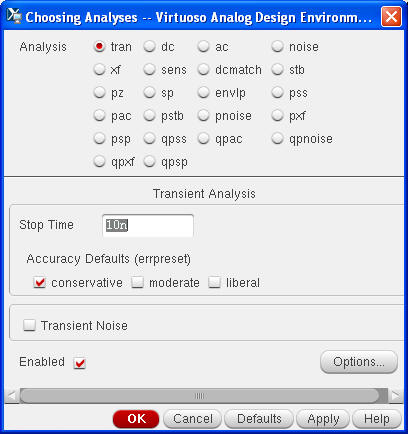
Choose an Analysis
- Use tran and set the stop time to be 1n (second is undersood)
For most of our labs we will use transient (tran) analysis, that is simulation of the circuits in the time domain. We need to set the stop time to be greater than the last interesting signal change in the design. We used a period of 1ns for the vpulse so this should show 10 cycles of the input.
- Check the "conservative" and Enabled boxes
Conservative gives the most accurate simulation with the highest computation cost. For large circuits one might not chose this.
Choose Outputs to Display
- Select Outputs -> to be plotted -> select on schematic.
Go back to the schematic window and click on wires to select them for voltage plotting, and click on nodes to see the currents going through a node
- Select the input and output wires for voltages and the power supply node into the inverter for current.
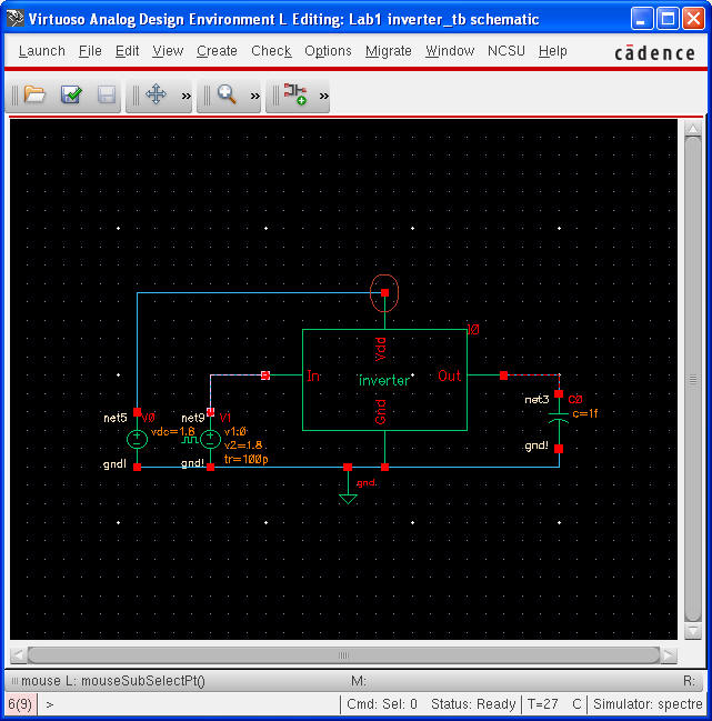
Those nodes will be shown in the Outputs list:
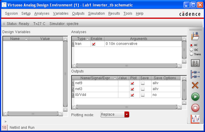
Now we are finally ready to simulate!
- From the ADE window menu, select Simulation -> Netlist and Run This will cause a simulation log file window to open to show you the progress of the simulation.
After your simulation has completed you should see the output waveforms:
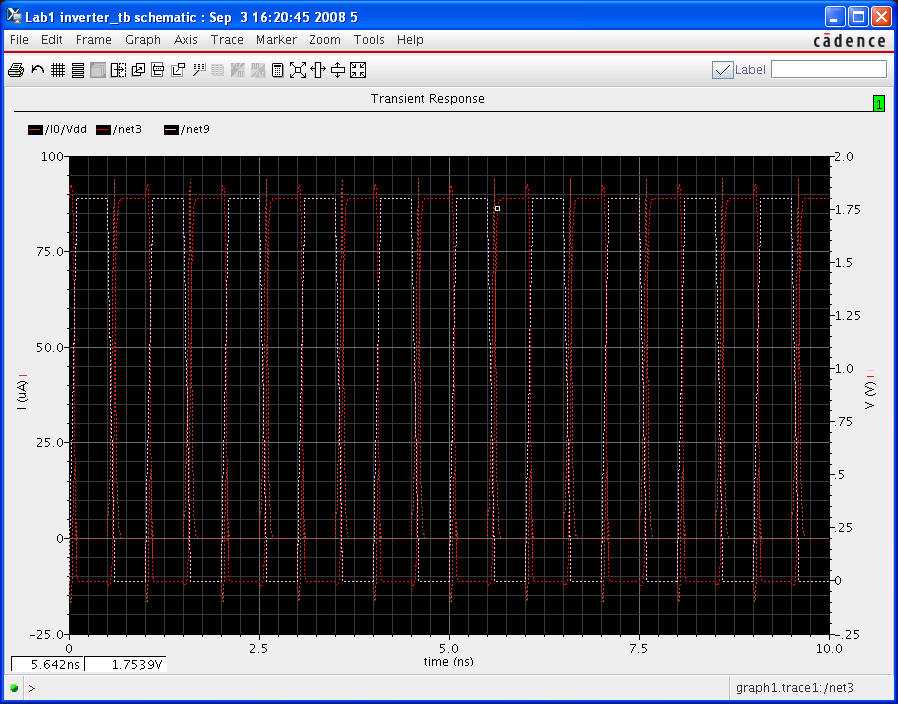
- You can change the background color by selecting separate the waveforms into individual plots using the Axis->Strips button on the menu
- Also you can change the color scheme by using the Frame ->Color Schemes -> White.
- Finally for each trace one can change the line style, color and thickness by selecting the trace and then right-clicking to get an edit menu.
There are lots of ways to zoom, compare and measure the waveforms
- You should play around with the measurement tools since they will be helpful in the coming laboratory assignments.
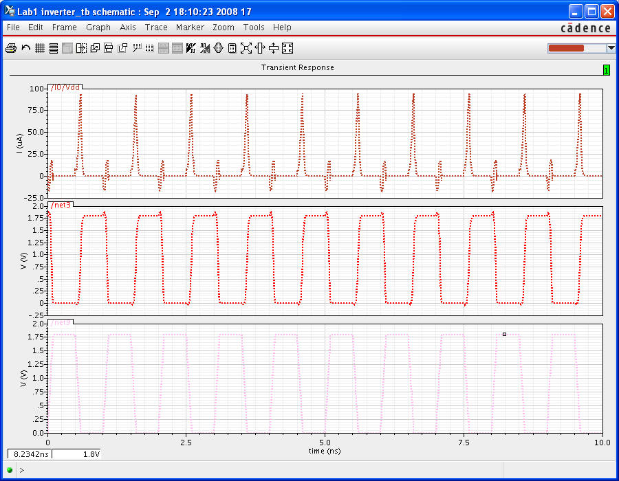
Here you can see the inverter inverts! And the current through the vdd node spikes on the rising edge.
Question: why doesn't it spike on the falling edge as well?
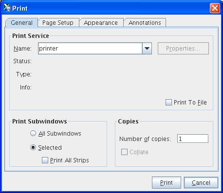
- To print out the waveform, select File->Print and in the pop-up window select printservice = printer